West Bengal Institute of Technology (WBIT) 2010-1st Year B.Tech Electronics and Communications Engineering WBUT Basic Electronics Engineering - Question Paper
CS/B.Tech/Sem-2/EC-201/2010
Basic Electronics Enginnering
Time Allotted : three Hours
Full Marks : 70
obtain the ques. paper attached beneath as a PDF.
Name :......................................................................
Roll No. : .................................................................
Invigilator's Signature : .................................................
CS / B.Tech/ SEM2 /EC201 /2010 2010
Time Allotted : 3 Hours Full Marks : 70
The figures in the margin indicate full marks.
Candidates are required to give their answers in their ot >n fjords
as far as practicable*
GROUP- A
( Multiple Choice Type Quest )
1. Choose the correct alternatives for any u-r of the following :
10 x 1 = 10
i) If the temperature of n- ;ype semi-conductor is increased then it becomes '
a} more n-type b) p~type
q]/ intrinsic d) none of these,
ii) Compared to avicmche diode, Zener diode has
a) less concentration
by less bariier field intensity
c) . hl$h-2T barrier field intensity
d) . higher depletion width.
iii) Forbidden energy gap of silicon at 0 K is a) 0-78 eV b) 1*2 eV c) 1*5 eV d) 0-3 eV.
iv) The major part of current flowing in an intrinsic semiconductor is due to the drift of
a)/ conduction band electrons
b) conduction band holes
c) valence band electrons
d) valence band holes.
v) The capacitance of a varactor diode can be changed by varying its
a) doping level b) temperature c) forward bias d) reverse bias.
vi) If a resistor hss *1 colour code yellow-violet-gold, the value of the rci?: jt is
47 Q b) 0-47 Q
c) 470 d) 4-7 Q.
vii) SC X xzny be turned off by
interrupting its anode current
b) reversing polarity of anode-cathode voltage
c) both (a) & (b)j
d) none of these.
vili) Voltage series negative feedback
a) increases input & output impedances
increases input impedance & decreases output impedance
c) decreases input & output impedances
d) increases output impedance & decrekes input impedance,
ix) In reverse biased condition junction capacitance of step graded PN-junction diode varies propers really
a) V'1'2 b) V'1/?
c) y1/4 d) i?one of these.
x) Without a DC source a clip;; was like a
*
a) rectifier t clamper
c) chopper d) demodulator.
xi) Integrated circuit acts; uS a/an
a) LPF b) HPF
c) BPF dj none of these.
xii) Output ironed;-nee of an ideal op-amp is
a) 0 b) 75 ohm
c) 100 k ohm d) none of these.
xiii) The value of CMRR for an ideal op-amp is
a) 0 b) 1
c) infinite d) none of these.
I Turn over
2001
3
xiv) The maximum efficiency of a full-wave rectifier can be
a) 37*2% b) 40-6%
c) 53-9% 81-2%.
xv) If the line frequency is 60 Hz, the output frequency of a bridge rectifier is
a) 30 Hz b) 60 Hz
c) 120 Hz d) 240 ii. .
GROUP -B (Short Answer Type )
Answer any three of tt, fallowing. 3x5= 15
2. Explain how Zener diode can Vc used as a reference voltage source.
3. Compare between an FI\T and a BJT.
4. Explain the working of an integrator circuit using ideal op-amp.
5. For wb&i tv:'pose is a triggering circuit provided in a CRO ? Expl&to :ow a CRO is used to measure the frequency of an alto? nating current flowing in a circuit.
6. An amplifier has a voltage gain of 200. The gain is reduced to 50 when negative feedback is applied. Determine feedback factor (3 and express the amount of feedback in dB.
GROUP-C ( Long Answer Type Questions )
Answer any three of the following. 3 x 15 = 45
7. a) What are the advantages of negative feedback ? 3
b) Explain with proper diagram the ccoiiguration of current series and current shunt fefvib?, jk circuit. 8
c) Distinguish among Class A, B and Push-pull amplifiers. 4
8. a) Write the working princ>* ;c of JFET with diagram. 6
i
b) Define TranscoAduMce, AC drain resistance, Amplification factor of JFET. 3
c) Draw the roircaon source JFET amplifier circuit and find oar the expression for voltage gain, input impe(/V.i< s and output impedance. 4
d) V-rrli-;r three differences between JFET and MOSFET. 2
9. a). Explain the Ebers-Moll Model. 5
b) What are the factors that affect the bias stability of a transistor ? 3
[ Turn over
2001
5
c) What is early effect ? 2
d) Draw the circuit diagram for self bias configuration considering an n-p-n transistor in the CE configuration.
Derive the expressions for its stability factors. 3 + 2
10. a) The metal lead of the p-side of a p-n is soldered to
the metal lead of the p-side of another p-n diode. Will the structure form an n-p-n travMstor ? Why ? 3
b) Draw the common emitter circuit of a transistor. Sketch its output characterIndicate the active, cut-off and saturation rvVSiorjs. 7
o
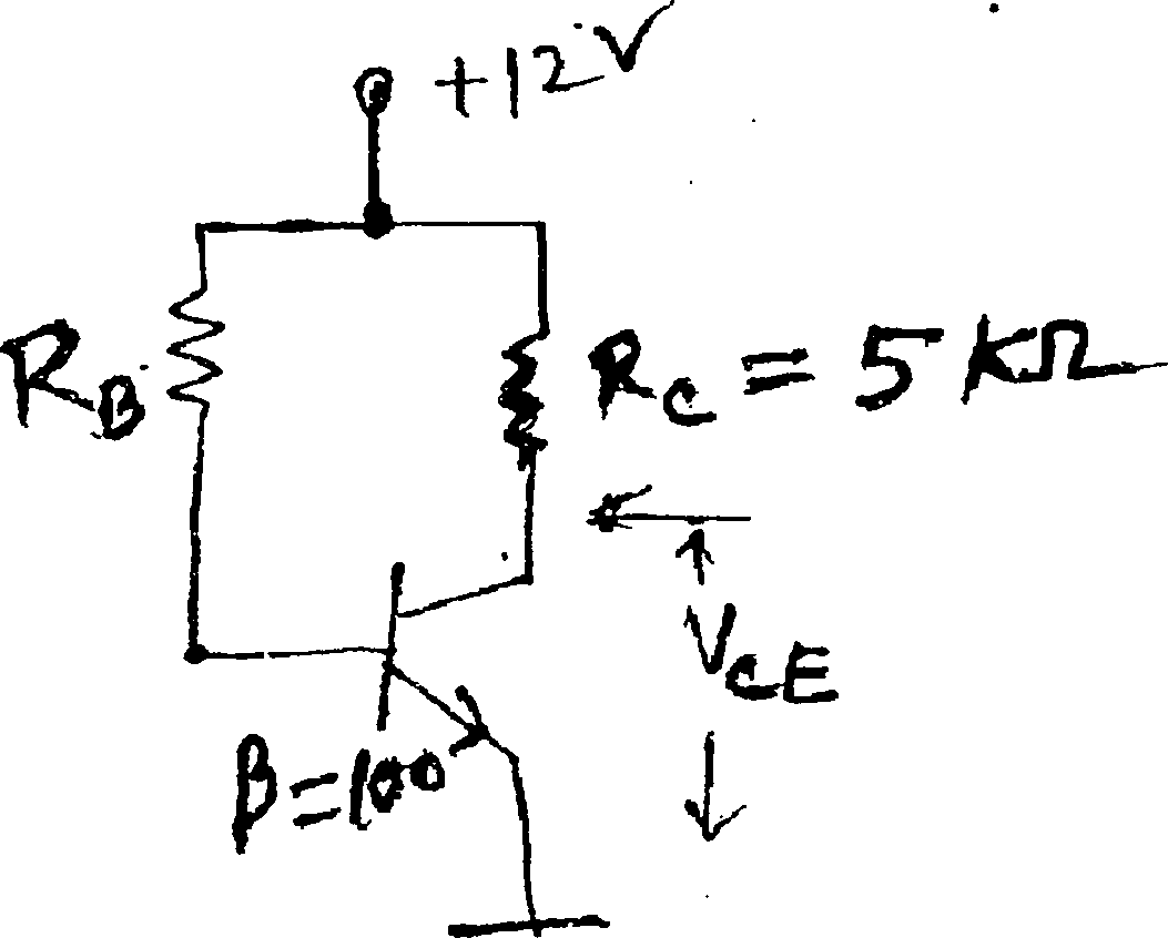
c) For a silicon BjT as shown in the following figure, find .RB to esbiUh V = 2 V. Assume VBE = 07 V, 5
CS/B,Tech/SEM-2/EC-201 /2010
11. Write short notes on any three of the following : 3x5= 15
a) Early effect
b) Clipper circuit
c) . UJT
d) Enhancement and depletion type CMOS
e) Hybrid parameters for a transisu.
2001 7
I
|
Attachment: |
| Earning: Approval pending. |