West Bengal Institute of Technology (WBIT) 2008-6th Sem B.Tech Electronics and Communications Engineering Electronics & Comm ( - ) VLSI Circuits & Systems - Question Paper
C8/B.TECHCBCE)/8EM-6/BC-604/08 3

ENGINEERING ft MANAGEMENT EXAMINATIONS, JUNE - 2008
SEMESTER - 6
Time: 3 Hours] [ FuU Marks : 70
GROUP-A (Multiple Choice Type Questions)
1. Choose the correct alternatives for the following : 10x1- 10
I) Pseudo NMOS logic provides which of the following advantages ?
a) Static power dissipation is less compared to CMOS logic
b) It is much faster compared; to other logics
c) It requires less no. of transistors compared to CMOS logic
d) It is more noise immune.
II) Frequency Compensation for an OP-AMP can be achieved by
a) increasing gain b) minimizing overall phase shift
c) adding a zero, d) none of these.
iii) Among the given OP-AMP topologies which one has the highest output swing ?
a) Telescopic b) Folded Cascaded
c) Two Stage d) Gain Boosted.
Iv) Typical value of subthreshold slope is
a) 80 mV/decade b) 60 mV/decade
c) 40 mV/decade d) 90 mV/decade.

v) Slant In ( occurs due to
a) body effect ;
velocity saturation mobility degradation.
v-i
(ohm)"1
c) channel length modulation
vlj) The unit for (HnCw) is
a) A/V2
c) ohm
e) No unit.
vii) To Implement the Boolean function F = A ( B + CD) using static CMOS design, number of transistors required is
a) 4 b) 8
c) 6 d) 12. [
viii) A logic gate has VOH = 5V, VOL = 0-2V, Vm = 2-5V and VIL = 0-8 V. The noise margins are
a) 0-6 V and 2-5 V b) 2-3 V and 4-2 V
c) 1-7 V and 2 3 V d) 1-7 V and 4-8 V. 1
ix) DRAM is widely used because .
a) refreshing operation is not needed
b) of low cost and high density
c) of low power consumption
. d) of high speed. _
x) The model parameter LAMDA (X) in a MOS structure stands for
a) Flicker noise coefficient
* b) Transit time
c) Channel length modulation
d) Transconductance. _
/ w *

<||P||kTBCH(KCE)/8EM-6/BC-604/08 5
GROUP-B
at- : ' ' ' h : '
( Short Answer Type Questions)
. ' ' . s
Answer any three of the following. 3x5=15
2. Design the following circuits using Transmission Gates : 2 x 2 ~
a) B-ttiQop - '
b) 2 input XOR Gate.
3. Explain how a combination of swlthches and capacitors can be used to emulate a resistor. , 5
4. Design a current sink of 30 fiA assuming the mirror transistor current is 10 |xA. Given -VDD = - Vgg = 2-5 V, VGS = 1-2 V and W/L ratio for the mirror transistor as 15/5. 5
* 1 ** ' ' '
5. Explain why NOR Gates are preferred for NMOS circuits while NAND Gates are
preferred for static CMOS circuits. 5
6. Describe the following pheomena In MOS structure : 2x2
0 Velocity saturation
b) Channel length modulation.
GROUP-C ( Long Answer Type Questions)
Answer any three questions. 3 x 15 = 45
7. a) Describe in detail Lamda-based design rule for layout design,
b) What Is stick diagram ? Mention its use.
c) What do you mean by active layer and poly layer In CMOS process ?
d) Write down the difference between twln-tub process and p-well process.
6 + 3 + 3 + 3
8. a) Draw the circuit diagram of dual slope A/D converter and explain Its operation.
b) What is a phase locked loop ? Mention two uses of phase locked loop.
c) Realize an active LPF of cut-off frequency 10 kHz and gain 10. 6 + 5 + 4
9. a> Draw the layout of a CMOS inverter ( not to scale J. Explain your drawtiig
conventions.
>

b) Design a static CMOS circuit to implement the Boolean function . F = D.JS.A + B.C.
c) Draw the circuit of a CMOS full adder circuit and explain its operation. 5 + 5 + 5
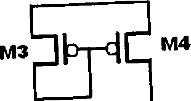
10. a) Explain with a circuit diagram, operation of a differential amplifier. -
b) What is CMRR ? Determine CMRR of the following circuit. .
|
V< |  |
* - 6+13+6)
11, a) Why is reference voltage required in IC ? What are the criteria for a good reference voltage source in VLSI circuit ? .
b) Explain the operation of a band gap voltage reference source in a VLSI circuit
c) Explain briefly difficult stages of an operational amplifier with the help of a block
diagram.
END
( 2 + 2 ) + 7 + 4
VI-389722 (S-A) |
|
Attachment: |
| Earning: Approval pending. |