Uttar Pradesh Technical University (UPTU) 2007-2nd Sem B.Tech Electronics and Communications Engineering 2006- ELECTRONICS ENGINEERING - Question Paper
Printed Pages : 7 TEC - 201
(Following Paper ID and Roll No. to be filled in your Answer Book)
Roll No. | | | | | | | | | 1 | B. Tech.
PAPER ID : 3034
(SEM. II) EXAMINATION, 2006-07 ELECTRONICS ENGG.
Time : 3 Hours] [Total Marks : 100
Note : Attempt all questions. All questions carry equal marks.
1 Attempt any four parts of the following : 5x4=20
(a) Describe the characteristics of ideal diode. Determine the ON and OFF state of the device.
(b) Draw the characteristics in foward and reverse bias and explain it.
(c) Show the energy levels diagram in insulators, semi-conductor and conductor materials.
(d) Differentiate between :
(i) Donor and acceptor impurities
(ii) Intrinsic and Extrinsic semiconductors.
(e) Explain the static and dynamic resistance in p-n junction diode. Determine the dc resistance levels for the diode of in following fig at
(i) ID = 2mA
(ii) ID = 20mA
(iii) vD = -10V
 |
Vi |
(f) Describe how diffusion and Transtition Capacitance differ. Draw the characteristics of Transition and diffusion capacitance versus applied bias voltage.
Attempt any four parts of the following
5x4=20
(a) What is dc load line? Prove that the operating point should be in the middle of the dc load line.
(b) Draw the circuit diagram of a full wave rectifier using two diodes and calculate
(i) Idc
(ii) Trms
(iii) PIV rating of diode.
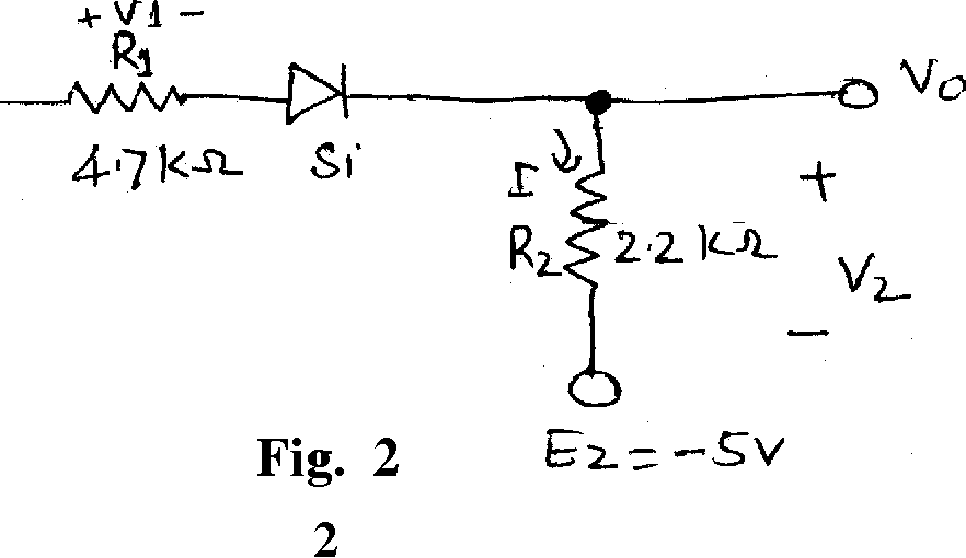
(c) Determine I, Vj, V2 and VQ for the series dc configuration of the following figure.
4
L
0-1
Cr
I
-gT
_ iPV
Fig. 3
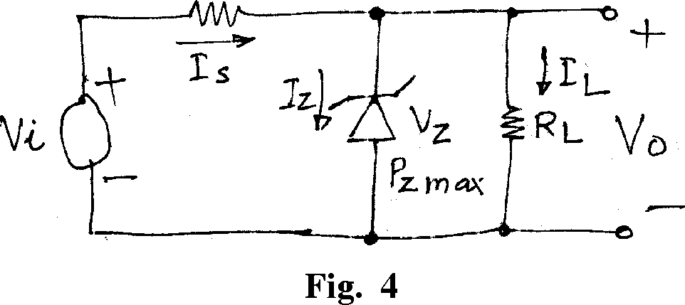
(e) Determine Is, IL and Iz.
|
Rs |
 |
|
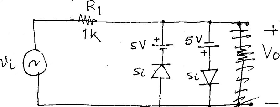
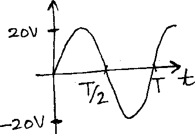
(f) Sketch the output waveform. |
Explain why a transistor action can not be achieved by connecting two back-to-back diodes. In a transistor explain, why emitter region is heavily doped, base width is small and collector area is large? Determine the following for the voltage divider configuration
(i) Ic (ii) VE (iii) VB (iv) Vc (v) Rj
(a)
(b)
|
+ !6V | |
 |
~ 80 |
Differentiate CB, CE and CC circuits.
(c)
(d)
Determine the resistor values for the following network for the indicated operating point and power supply voltage. y Vcc
 |
ac ca*\ C e - fit |

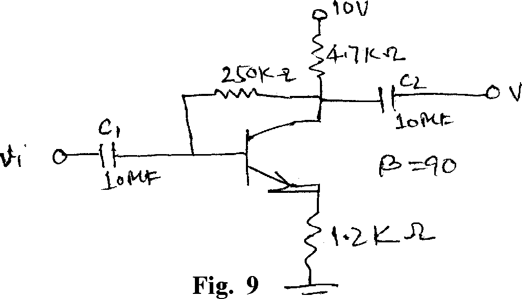
(1) Determine the quiesent levels of Ic2 and VCEq for the network
4 Attempt any two parts of the following : 10x2=20
(a) Draw the structure of a JFET and explain its principle of operation with neat diagrams. Also sketch its V-I characteristics. Define pinch-off voltage and mark it on the characteristics. Explain its importance.
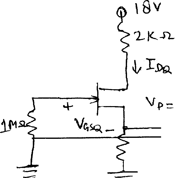
(b) For the given measurement Vs = 1.7V for the network as shown in the figure determine.
|
(i) |
IDq |
|
VGSQ | |
|
(iii) |
I)SS |
|
(iv) |
vD |
|
(v) |
vDS |
(c) Describe briefly, the construction of a MOSFET in enhancement, mode. Draw its characteristics. Draw the equivalent circuit of a MOSFET operating in enhancement, mode.
 |
4V 0*l |<LJL |
|
Fig. 10 | |
10x2=20
Attempt any two parts of the following :
(a) (i) Convert the following numbers
(a) (6089.25)10 = (
(b) (A6B.F5)16 = (
(c) (375.37)8 = (
(ii) (1) (A4F.EF)16
+ (3FD.AB)16
(2) (6488.43)9
- (3837.78)9
(3) (F A I 2.35)16 -(9 BCD.EC)16
(iii) Simplify the following logic expression using Boolean algebra
(a) f = AB + A (B+C) + B (B+C)
(b) f = A BCD + ABD + BCD + AB + BC
(b) (i) Simplify the following expression using
K-map and implement the output using fundamental gates.
f (A,B,C,D) = (1,3,4,6,8,9,11,13,15) + d (0,2,14)
(ii) Simplify the following expression using K-map
f (A,B,C,D) = nM (0, 1, 3, 6, 7, 8, 9, 11, 13, 14, 15)
(c) (i) What are the properties of an ideal
operational amplifier used in measurement and instrumentation system? Explain with the help of circuit diagrams how it is used as
(a) Adder (b) Subtractor
(c) Integrator (d) Differentiator
(ii) Calculate the output voltage of an
OP-AMP summing amplifier for the following sets of voltages and resistors.
Use Rf = 1M fi in all cases.
(a) Vx = +1V V2 = +2V, V3 = +3V R!=500KQ r2=imq r3 = imq
(b) Vx = -2V, V2 = + 3V, V3 = +1V
Rx = 200 KQ, R2 = 500 KQ, R3 = 1MQ
V-3034] 7 [ 27650 ]
|
Attachment: |
| Earning: Approval pending. |