Bengal Engineering and Science University 2007 B.E Electrical Engineering Solid State Devices and Circuits-I - Question Paper
Ex/BESUS/ EE-404/07
B.E. (EE) Part-II 4th Semester Examination, 2007
Solid State Devices and Circuits-I (EE-404)
Time : 3 hours Full Marks : 70
Use separate answerscript for each half. Answer SIX questions, taking THREE from each half. Two marks are reserved for neatness in each half.
FIRST HALF
(to K-
1.
A/vYv Ri
A BJT transistor circuit is shown in Fig.l. Represent the circuit by replacing the transistor with its Ebers-Moll model. Given that aF=0.96, aj = 0.1, |Icol= 10nA, | IE01=1.1 nA. Volt-equivalent of temperature (VT) = 0.026 V, base-emitter voltage drop vBE = 0.75 V. Find iB, ic and iE. Find also Large signal a (alpha) and p (Beta) of the transistor. What is the collector voltage with respect to base?
[3+4+2+2J
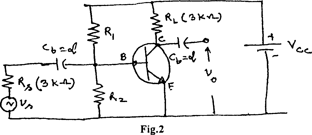
A CE BJT amplifier is shown in Fig.2. The h-parameter values are h,e = 1,100 Q, hre = 2.5 x 10⁻⁴, hfe = 50 and l/hoe = 40 kQ. Find the voltage gain and the current gain of the amplifier. Neglect the effect of biasing circuit. If a capacitor of infinite capacitance is connected between collector and emitter, find the voltage gain and current gain of the circuit. [4+3+2+2]
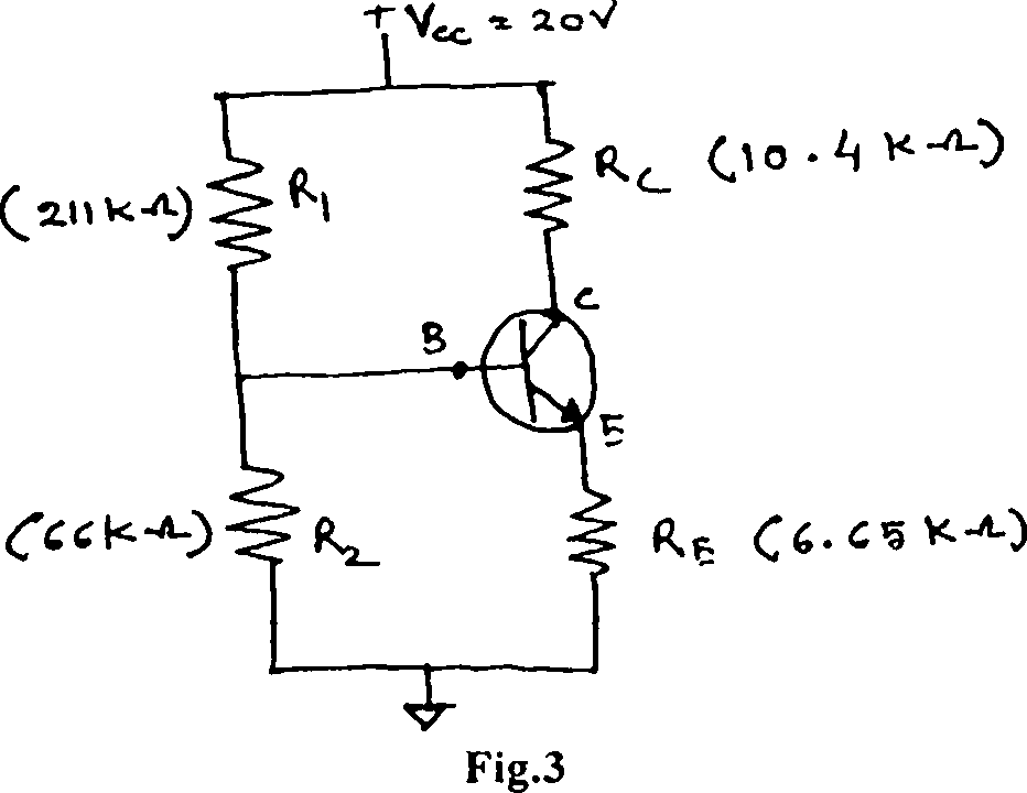
A biasing circuit is shown in Fig.3. The variation of VBE is 0.65 V to 100 mV, variation in Ico is 50 nA to 1000 nA and variation in p is 100 to 1000. Find ICq taking minimum values of VBE, Ico and p. Calculate change in collector current from the quiescent value due to simultaneous increases of VBE, Ico and p from their minimum value to maximum value. |4+7]
Deduce the expression of voltage gain and output resistance of a JFET CD amplifier. Draw a circuit diagram to illustrate a JFET CG amplifier. In which of the two amplifiers, the input resistance is more? [5+3+3]
5. Write short notes on any two :
[5'/2+5'/2]
i) Gate-source pinch-off voltage
ii) Current saturation in JFET
iii) Inverter logic circuit using CMOS
iv) Universal Biasing circuit for FET.
SECOND HALF
6. a) What is an operational amplifier (op.amp)? What is an ideal op.amp? With
the help of its equivalent circuit compare these two op.amps.
b) Draw the circuit diagram of a differential input differential output amplifier with the help of two op.amps and find the (differential) gain of the circuit.
c) Draw the circuit diagram of a non-inverting gain amplifier with gain more than unity and find the expression of gain. [4+4+3]
7. a) What is an integrator? With the help of circuit diagrams express input output
relation of (i) passive- and (ii) active- integrators using RC components. Compare the two.
b) What is a regenerative analog comparator circuit? Draw its transfer characteristics and label the important nodes in the diagram.
c) Using regenerative comparator and RC components, draw the circuit diagram of a square wave oscillator using op.amp and develop the expression of time period of output. |3+4+4]
8. a) A logic system is described with the help of a min-term expression as follows :
Y(A, B, C, D) = Zm(0, 5, 11, 14) + d(l,4, 7, 10, 13, 15)
Find out the minimal logic expression and realise the system with the help of AND-OR configuration.
b) The function of a Three-input (A, B, C) digital system (Y) is described as Y(A, B, C) = nM(l,0).
Draw its (i) truth table; (ii) Venn diagram; (iii) K-map; (iv) min-term (SOP) expression (extended); (v) Now minimise the logic system with the help of K-map to have its minimised SOP expression; (vi) Verify the minimal expression of the above system with the help of QMC-method of minimisation; (vii) Now using NAND-NAND configuration represent the minimal logic circuit of the system; (viii) Also draw the realised logic system using single 4 line -1 line MUX. |3+8|
9. a) What is a multiplexer? Draw the internal logic circuit of a single 4 line -1
line multiplexer (without STROBE).
b) Represent a 2-in XOR gate using four (4) 2-in NAND gates and show its performance analytically.
c) Realise a 2 - bit word squarer with BCD output using only an inverter and two 2-in AND gates. [4+4+31
10. Write technical short notes on any two : [S'/a+S'/j]
a) Any two active analog subtractor circuit using op.amps.
b) Three input adder circuit and its I/O relations.
c) An astable multivibrator using Op.amp.
d) TTL NAND gate with Totempole output and open collector output.
e) N-Ch MOS inverter and CMOS inverter.
f) Full Adder circuits and its use in a 4-bit parallel adder.
|
Attachment: |
| Earning: Approval pending. |