How To Exam?

a knowledge trading engine...


Anna University Coimbatore 2010 B.E Electronics & Communication Engineering Electronic circuits i - i - Question Paper

Wednesday, 16 January 2013 07:30Web


ELECTRONIC CIRCUITS I -NOV I DEC 2010

e>1

-?ca9'

ANNA UNIVERSITY OF TECHNOLOGY, COIMBATORE B.E. I B.TECH. DEGREE EXAMINATIONS : NOV I DEC 2010 REGULATIONS : 2008 THIRD SEMESTER 080290011 - ELECTRONIC CIRCUITS I (COMMON TO ECE I MEDICAL ELECTRONICS)

e>1

-?ca9'

Max.Marks : 100

Time: 3 Hours


PART - A

e>1

-?ca9'

(20 x 2 = 40 MARKS)

ANSWER ALL QUESTIONS

1.    What do you mean by faithful amplification?

2.    What are the three operating region of BJT?

3.    What are temperature dependent parameters in transistor?

4.    What is thermal runaway?

5.    Give four advantage of h - parameter method for analyzing transistor amplifier over other types.

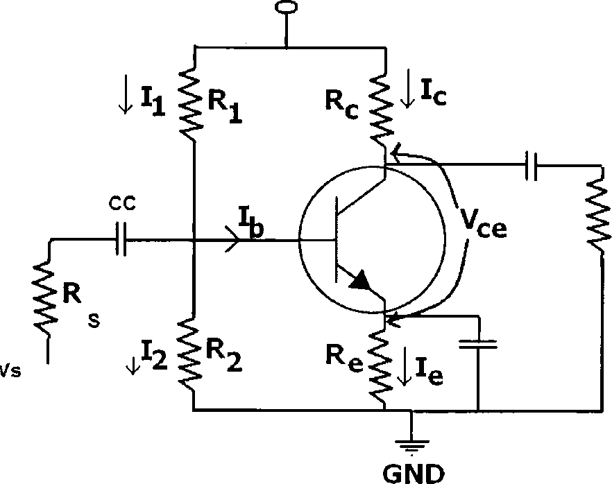
6.    Consider CE amplifier with fixed bias. If (B = 80,RB = 390 KQ, Rcl .5 KQ & Vcc =

30 V. Find the coordinates of Q-point.

7.    What is the role of coupling network in multistage amplifier?

8.    State Millers Theorem.

9.    Draw the High frequency model of FET.

10.    How the constant current circuit is used to improve the CMRR?

11.    Draw the high frequency equivalent circuit for BJT amplifier.

12.    Give the main reason for the drop in gain at the low frequency region and high frequency region.

13.    Compare the efficiency of class A, and class B amplifiers .

14.    How are amplifiers classified based on the biasing condition?

15.    How the conversation efficiency occurs?

16.    How the crossover distortion occurs.

17.What    is meant by ripple factor?

18.    A full wave rectifier delivers 50 W to a load of 200 Q. If the ripple factor is 1 %. Calculate the A.C ripple voltage across the load.

19.    Define line and load regulation.

20.    Give any four advantages of SMPS.

PART -B

(5x12 = 60 MARKS)

ANSWER ANY FIVE QUESTIONS

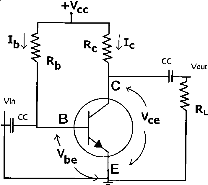
21a. In the transistor amplifier shown in figure 1, RC=10KQ, Rb=1 KQ RL=24KQ and Vcc = 24 V.    '

Draw the DC,AC load line and determine the optimum operating point.    (6)

Figure 1


1

b. Discuss the bias compensation in diode.    (6)

22.    Draw a voltage divider bias circuit and derive an expression for its stability factor.

Give the advantage of voltage divider bias over other types of biasing.

23.    Consider a single stage CE amplifier with Rs=1 KQ, 1=50 KQ, R2=Re =Rc=2 KQ, 1

Rl=2 KQ, hfe=50, hie=1.1 KQ, hoe=25 pA/V & hre =2.5 X 10'4. Find A,, R, Av, Avs, A,s &R0. Use approximate analysis if permissible.

+VCc

24.    Explain the function of differential amplifier with neat circuit. Derive its Ad, Ac and CMRR.

25.    Discuss the effect of emitter by pass capacitor on low frequency response of BJT amplifier.

"\

26. a. Draw the circuit diagram of a push pull amplifier and explain its working,

b. Derive the equation for efficiency of a class B amplifier.

27.    Write short notes on :

(6)


i)    Harmonic distortion

ii)    Frequency distortion

iii)    Phase distortion

28.    Explain the working principle of full wave rectifier circuit with n filter. Derive its ripple factor.

END*****

4


Attachment:

( 0 Votes )

Add comment


Security code
Refresh

Earning:   Approval pending.
You are here: PAPER Anna University Coimbatore 2010 B.E Electronics & Communication Engineering Electronic circuits i - i - Question Paper