North Maharashtra University 2011 B.E Computer Science and Engineering .s.ecomputer - university paper
THIS IS THE examination PAPER OF ANALOG ELECTRONICS OF second YEAR COMPUTER ENGINEERING.

1tz - 01

P Pages:3 Time: 3 Hours
Max Marks 100
Instructions ; I) Do not writ* anythmgon qucuum paper exit pi S*ai Vo
2) Answer any two fr<: $ach Unit AU units are compuitory
3) Assume suitable d.< \if necessary
V
4) Draw diagrams n/ztpcr necessary.
5) Figure. to right interne full marks
6) Use of non pni\;r<j calculator it alJowed

I
lNU
I. A) State and prove maximum power tranjfr r theorem for DC circuits
10
# *
B) Find out current through 200 resistor A>Ing Thevenins theorem for Figure (I > 10
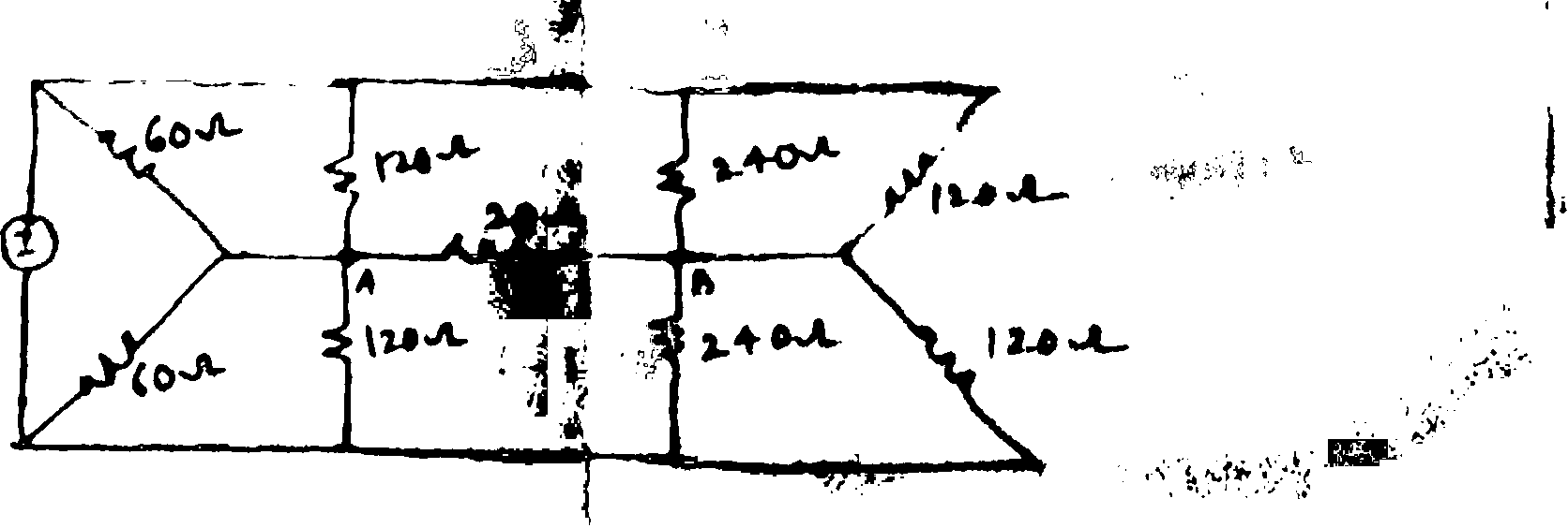
O Explain principal of duality, lindna! of circuit shown in Figure (I I); lo

II -II
I*
1 /) Draw circuit for common base contrition Derive expression for A,. Rj. A A 10
B) A voltage source of internal re*i**ar.c Rs - I kQ, drives CC amplifier using
Rt == 2 kfl, the CE h-parameter* we h- l.2kQ,hre = 2 * 10'4,hfc60,
* 25 n A/v. Calculate A,, R|t Ay., Ay. 10
C) Explain Millers theorem and its <|pl with neat diagram 10
I -III
3. A) Draw circuit diagram for class A senjt fed direct coupled amplifier, show that
maximum efficiency is 25%. , 10
B) Explain working of differential ampljflv with neat diagram in common and differential mode, drive the equatiorj for Ad only 10
C) Draw darlington transistor circuit. ijfplain what is boot strapping circuit and explain it. Also give the reason for it| requirement. I0
4. A) Explain self bias method for JFE1

UNIT-IV
B) Explain the stability of gain for sv gattvc fccdback Explain how it is more
stable by using negative faadbnck 10
4?) Explain working of Wien bridge o.villator Design the oscillator circuit to giv o/p frequency of 5 kHz use c 0.1 10
' "6
y ' p
wf ;r.
I
'WZU,'.'
5, A) Explain the action of zener regulator uiHjvirying load condition, for a zener regulator shown in Figure (III). Calculatpminimum and maximum load current Also calculate minimum load resistance If Y7 10 V. V, m 5 mA


f * t. Illlfl 1
 |
|
I |
10
$
Figure( 4*
t
i
B) Explain fold bock protection method t'fevoltage regulators
10
I
C) Design a regulator circuit using IC 72 having VQ 6.3 V, 100 mA,
|
V<rf-7V,V-0.7VuseR2 Draw designed circuit |
 |
|
Attachment: |
| Earning: Approval pending. |