National Institute of Technology 2006 B.Tech Production Engineering Pulse and Digital Circuits - Question Paper
Monday, 04 February 2013 12:40Web
Page 1 of 2
EE221 T PULSE AND DIGITAL ELECTRONICS – FEB 2004
TUTORIAL SESSION three (15-3-2004 3:00 PM to 5:00 PM)
COVERAGE – MODULE II of the Syllabus
1. A square waveform moving ranging from 0V and +10V with 50% duty ratio and 1Mhz frequency is available. A learner wants to use this source as the input to a TTL Inverter gate that he wants to test. He connects a potential divider using 2 100k resistances and connects the center point to TTL gate input. What is the output waveform that he will observe ? And what is the waveform that will appear at the potential divider output ?
2. A TTL Inverter gate is driven at the input by a 0V to 5V square wave of 50% duty ratio and 1MHz frequency.The gate is said to have 10 ns propagation delay in both directions under unloaded conditions. A learner tries to measure the propagation delay in the oscilloscope. Estimate the propagation delays that he will measure.
3. The learner in the above issue wanted to step down the TTL output to 1V amplitude. He tried a 270k+100k potential divider and observed the voltage across the 100k resistance using an oscilloscope.He saw a waveform which was almost d.c. discuss why and estimate the magnitude of d.c voltage that he observed.
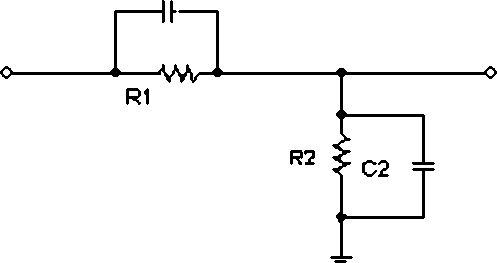
4. Find the transfer function of the circuit beneath and obtain the condition that will ensure that the transfer function is a real number.
5. C1 in the above circuit is a variable capacitance. R1 = 9M , R2=1M. C2 is around 20pF and is the oscilloscope input capacitance but is not accurately known. Evolve an experimental procedure using a square wave at the input and an oscilloscope at the output to adjust C1 to the right value.
6. One input of a standard TTL Nand Gate is held high. The other input is provided a 0 to 5V square wave at 1Mhz. It is obtained that the gate runs hotter when the rise time and fall time of input waveform is increased from an initial value of 5ns to 50ns. discuss why? Will the power supply avg. current depend on the rise and fall times of input waveform?
7. One input of a standard TTL Nand Gate is held high. The other input is provided a 0 to 5V square wave at 1Mhz. The input wave has negligible rise and fall times. The output of this gate is provided to the input of a different similar gate. Which gate takes higher avg. supply current? Why? Which gate runs hotter and why?
|
Attachment: |
| Earning: Approval pending. |