National Institute of Technology 2007-3rd Sem B.Tech Electronics and Communications Engineering ECU 202 : LOGIC DESIGN – - Question Paper
Sunday, 03 February 2013 11:05Web
Page 1 of 2
NATIONAL INSTITUTE OF TECHNOLOGY, CALICUT
Third Semester B.Tech End Semester exam – November 2007
ECU 202 : LOGIC DESIGN
Time: three hrs. Marks: 50
ans All ques.
1 Four Chairs are placed in a row:
A B C D
every chair may be occupied (“1”) or empty (“0”). provide the minterm and maxterm expression for every logic function defined beneath and then minimize the maxterm
expression of every function to get the simplified logic functions in POS form.
a) F (A,B,C,D) is one iff there are no adjacent empty chairs.
b) H (A,B,C,D) is one iff at lowest 3 chairs are occupied.
c) J (A,B,C,D) is one iff there are more people sitting in the left 2 chairs than in the right 2 chairs.
[Marks 6]
2 It is necessary to design a decimal adder for 2 digits represented in the excess-3 code. Construct the adder with 2 four – bit parallel adders and necessary logic gates. Output of the adder should be also in excess-3 format.
[marks 4]
3 Implement a Full Adder :
a) Using 2 8:1 MUXes. Connect X, Y & Cin to the choose inputs of the MUXes and connect one or 0 to every data input.
b) Using 2 4:1 MUXes and 1 inverter. Connect X & Y to the choose inputs of the MUXes and connect 1’s, 0’s, Cin or to every data input.
c) Again using 2 4:1 MUXes, but this time connect Cin & Y to the choose inputs of MUXes and connect 1’s, 0’s, X or to every data input.
[marks 3]
4 a) Draw the circuit of a simple JK flip flop using NAND gates. [marks 1]
b) find its truth table [marks 1]
c) What is Race Around problem? Mention 2 methods for eliminating this issue [marks 2]
d) Draw the replaced JK flip flop with no race around issue [marks 1]
.
5 Braille is a system which allows a blind person to learn alphanumeric by feeling a trend of raised dots. Design a circuit that converts BCD to Braille. The table one indicates the correspondence ranging from BCD and Braille. Use a PLA. provide the PLA Table.
[marks 3]
A B C D
0 0 0 0 •
• •
0 0 0 1 •
0 0 1 0 •
•
0 0 1 1 • •
0 1 0 0 • •
•
0 1 0 1 •
•
0 1 1 0 • •
•
0 1 1 1 • •
• •
1 0 0 0 •
• •
1 0 0 1 •
•
6 An MN flipflop works as follows: if MN = 00, the next state of the flip flop is 0, If MN = 01, the next state of the flip flop is the identical as the current state, if MN = 10, the next state of the flip flop is the complement of the current state, if MN = 11, the next state of the flip flop is 1
a) find the excitation table of the FF [marks 1]
b) Using MN flip flops design a three bit synchronous counter which counts in the subsequent sequence : 000, 001, 011, 111, 101, 100 (Repeat) 000, ………. [marks 3]
7 Design a four –bit shift register using four D flip flops, four :1 MUXes and additional logic gates to operate according to the subsequent table:
Inputs Next State Action
S1 S0 Q4(n+1) Q3(n+1) Q2(n+1) Q1(n+1)
0 0 Q4 Q3 Q2 Q1 No change
0 1 Serial input Q4 Q3 Q2 Right Shift
1 0 D4 D3 D2 D1 Parallel Load
1 1 Q1 Q2 Q3 Q4 Reverse Bits
[marks 3]
8 A synchronous counter is needed to count up from 010 to 1010 through the even numbers and then down to one through the odd numbers – ie., the sequence 0,2,4,6,8,10,9,7,5,3,1,0……. Design the counter using T kind flip flops.
[marks 3]
9 a) Generate the subsequent Random Sequence using a shift register and necessary logic gates:
S = • • • • one 0 one 1 one 1 0• • • • [marks 3]
9 b) The decimal equivalent of the largest number a binary ripple counter can count is 4095. What should be the clock frequency at the input to the counter if it is necessary to find a frequency of 550 Hz at the output of the most significant stage ? Neglect propagation delays. [marks 1]
c) A ripple counter is to be constructed using flip flops with propagation delays 35 ns. If the counter is to be clocked at two MHz, what is the maximum modulus of the counter? [marks 1]
d) Construct a truth table for the circuit shown below: diagram 1 [marks 2]
10 a) presume a stream of 50 k bits are provided to the circuit whose output Z=1 when number of 1’s in 50 k bits are odd else Z=0. Design the circuit using Mealy FSM. [marks 2]
b) Design a FSM to detect a sequence “101” (overlapping & non-overlapping) using D flip flops. [marks 3]
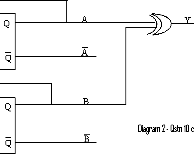
c) find the state table and state diagram of the Moore FSM provided below: diagram2 [marks 2]
11 a)Briefly discuss the subsequent terms associated with Digital Circuits:
i) Set up time
ii) Hold time
iii) Clock skew
iv) Static & Dynamic Hazards [marks 2]
b) obtain a circuit that has no static hazards and implements the Boolean function
F (A,B,C,D) = ?(0,2,6,7,8,10,12) [marks 3]
R |>X>-C>0D*>
--
s-
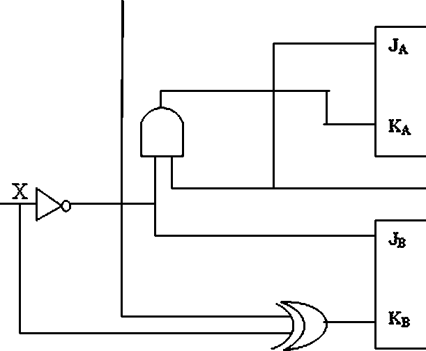
Diagram 1-flstii 9 d
|
Attachment: |
| Earning: Approval pending. |