National Institute of Technology 2004 B.Tech Electronics and Communications Engineering EE 221 T PULSE AND DIGITAL ELECTRONICS - Question Paper
Please obtain the attachment
1.
NATIONAL INSTITUTE OF TECHNOLOGY , CALICUT
FOURTH SEMESTER B.TECH. (ENGINEERING) DEGREE EXAMINATION, APRIL 2004 EE 221 T PULSE AND DIGITAL ELECTRONICS :Three Hours Maximum : 50 Marks
Time
PART - A (Answer All)
Explain the operation of symmetrical triggering circuit employed in triggering a transistor bistable multivibrator circuit.
Explain the basic principle of Miller Voltage Sweep System and derive an expression for its sweep speed error taking into account the non-idealities of the Amplifier used.
2.
3.
4.
5.
6.
7.
8.
1
What is meant by active pull-down in a TTL circuit? Explain the performance improvements obtained by using active pull down.
How does the power dissipation of CMOS gates vary with (i) input frequency (ii) load capacitance and (iii) supply voltage? Explain.
Design an EXNOR Gate using (i) only NAND gates (ii) only NOR Gates.
What is a PAL? Explain how combinational logic can be implemented using a PAL with an example.
Show the realization of a clocked master-slave JK flip-flop and explain its operation. How is a master-slave JK FF superior to a simple JK FF?
Draw the diagram of a 4-bit natural binary synchronous up/down counter using JF flip-flops. Explain how such 4-bit counters can be cascaded.
(8 x 2 = 16 Marks)
PART - B (One from each OR pair)
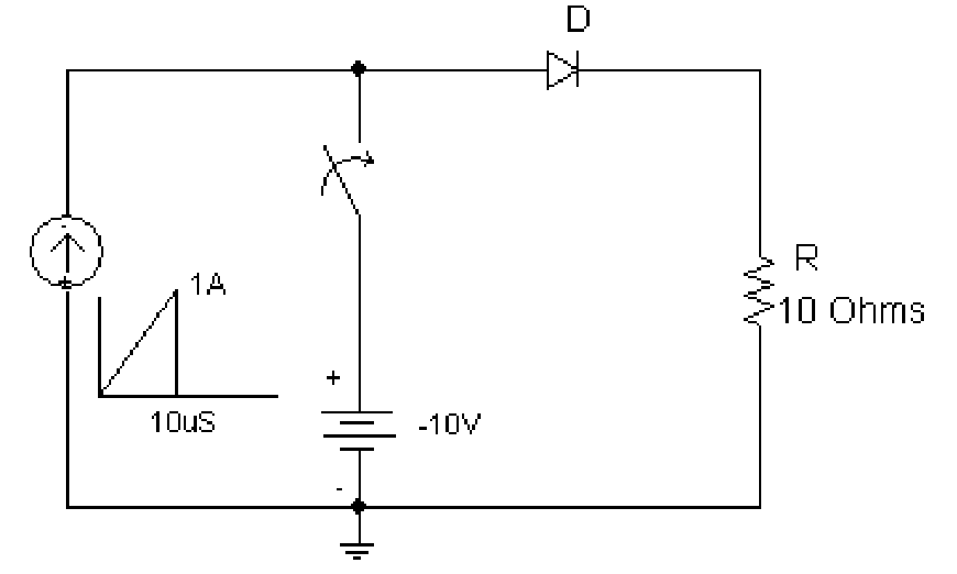
The diode in the figure below has a storage time constant of 3|js and transition capacitance of 1nF.The switch is closed at t=15us. Calculate and plot the minority charge storage in the diode, diode current, voltage across diode and voltage across resistor from t=0 to t=25us. (6 Marks)
OR
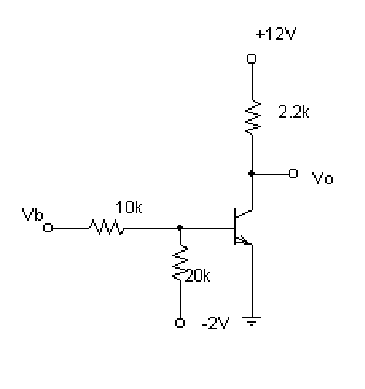
The input wave in the figure below is a 200kHz square wave with 6V high level and 0 V low level. The transistor parameters are pmin = 70, CTe = 4 pF, Cc = 7 pF, rbb' = 30 ohms, ts = 350ns and fT = 7.5MHz. Find all the components of switch-off delay and switch-on delay of the transistor and draw the output voltage waveform showing the various switching delay components. (6 Marks)
3 Explain why (i) Standard TTL is faster than standard DTL (ii) Schottky TTL is faster than standard tTl (iii) TTL Supply Current contains spikes (iv) Flip Flops draw more supply current when clock waveform rise and fall times increase (v) ECL uses negative supply and (vi) Speed-power product is used as a figure of merit in comparing digital logic families (6 Marks)
OR
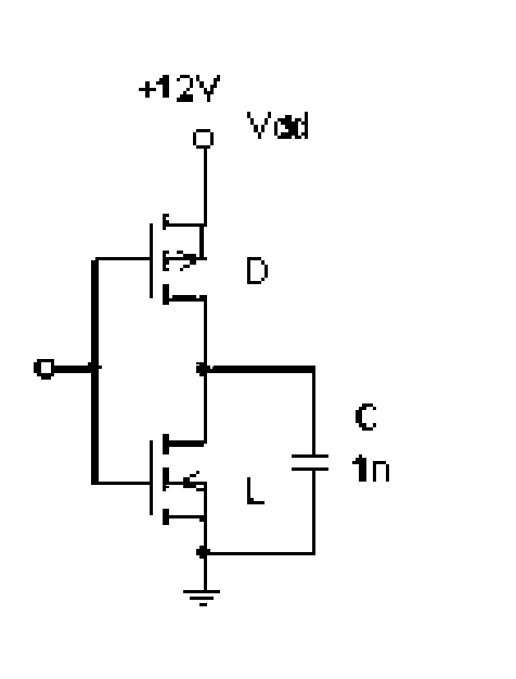
Derive expressions for the rise time and fall time for a CMOS Inverter driving a capacitive load as shown in the figure below. Evaluate the rise time and fall time for kD = 1 mA/V2 , kL = 1.3 mA/V2 , VTn = 2.5V , VTp = 2 V and C = 1nF assuming an ideal square wave input at the input of the gate. (6 Marks)
4
5(a) Explain how Combinational Logic may be implemented using a ROM. Illustrate the procedure by designing a ROM Implementation for a circuit which accepts a 3-bit number and generates a binary number which is equivalent to x3 + 2 where x is the decimal equivalent of the 3 bit input. (5 Marks)
5(b) For the function F(a,b,c,d) = 2(2,5,11,15) and X(a,b,c,d) = 2(1,3,4,6,7,8) where X(a,b,c,d) represents don't-care conditions find (i) Two level NAND realization by minimizing F by K Map
(ii) Two level NOR realization by minimizing F' by K Map and applying De Morgan's theorem on the resulting function (iii) Three level NOR realization by minimizing F by K Map , complementing both sides of the resulting function and applying De Morgan's Theorem on
R.H.S (you will need an inverter at the third level to get F from F' ) (iv) Three level NAND realization by minimizing F' by K Map , and using an inverter in the third level. (6 Marks)
OR
6(a) Implement the following Boolean Functions with an 8 X 1 multiplexer. (5 Marks)
F1(A,B,C,D) = X (0,3,4,6,8,10,12,13,15)
F2(A,B,C,D) = n (0,3,5,6,7,10,11,13,14)
6(b) (i) Design a one-bit comparator circuit using only NAND gates. (ii) Using one-bit magnitude comparator as the building block construct a 4-bit magnitude comparator. Use NAND gates for interconnection as required. (6 Marks)
7(a) Draw the internal diagram of an edge-triggered D flip-flop and explain how edge triggering is achieved in this flip-flop. Also, explain the significance of setup time and hold time. (5 Marks)
7(b) Design a mod-9 Binary Counter using detect and steer' method. Use JK Flip-flops. Explain how you take care of the unused states in the counter. The counter should be self-correcting (6 marks)
OR
8(a) Draw the schematic diagram of a 4-bit bidirectional shift register with parallel load feature and explain its operation. (4 Marks)
8(b) Design a counter with JK flip flops by excitation table method to satisfy the specification -when an input x' is 0 the counter should cycle through 000->001->010->100->000 and when the input x' is 1 the counter should cycle through 000->001->011->111->110->100->000. The counter must be self-correcting. (7 Marks)
|
Attachment: |
| Earning: Approval pending. |