National Institute of Technology 2010 B.Tech Kurukshetra Basic Electrical Engg(BEC) . - Question Paper
NATIONAL INSTITUTE OF TECHNOLOGY, KURUKSHETRA
THEORY EXAMINATION Month and year of the Examination: May/June, 2011 Programme: B.Tech Semester: 2nd
Subject: Basic Electronics Engineering
Course No.: ECT-103 Maximum Marks: 50
Number of Questions to be attempted: Five Times allowed: 3:00 Ilrs
Total No. of Questions: Eight Total No. of Pages used: 2
NOTE: Attempt Five questions in all selecting at least one from each unit.
Unless stated otherwise, the Symbols have their usual meanings in context with the Subject. Assume missing data required, if any. The Candidates, before starting to write the solutions, should please check the Question Paper for any discrepancy, and also ensure that they have been delivered the Question Paper of correct Course No. and the correct Subject title. ___
Ql.
3
2
|
5- |
 |
T
(f)ZA
UNIT I
(a) In a series RC circuit, the current and voltage are given as:
I = 2cos (314tf-10), V = lOcos (314ttJ-20). Determine the values of R and C.
(b) Explain in detail the Metal film resistors.
(c) Apply superposition theorem to determine the voltage across the IQ resistor for the circuit shown in fia. 1.
|
V | ||||||||||||
|
w l |
\ O V |
1 | ||||||||||
|
)ZV |
F T (a) For the periodic waveform shown in fig.2, calculate the RMS value, average value and ripple factor. Q2. (b) Find the current in 3Q resistor for the circuit shown in fig.3. (c) Find the current in series RC circuit having R = 20f2 and C = lOnF to which a dc voltage of 10 V is applied at t = 0. Determine the .value of this current at the instant t = 2 msec. lit 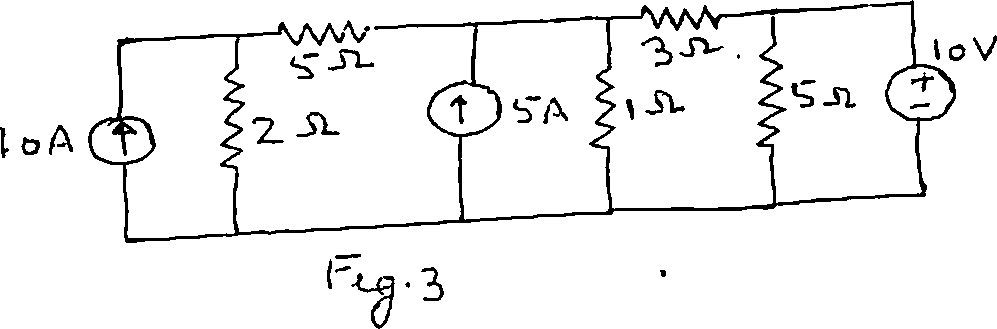
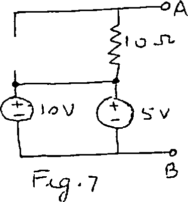
\TJua.li Q.3 5 3 Q.4 4 (a) Write a short note on mica capacitors. (b) Use Norton theorem to determine the voltage V for the circuit shown in fig.4. (c) How can a voltage source be converted into a current source and vice-versa? (a) Find the equivalent inductance of the network shown in fig.5. All inductors are of 5H each. (b) Determine the capacitive reactance and total impedance for the circuit in fig.6 at resonance. Also calculate resonant frequency and Q factor. (c) Determine the voltage across terminals AB in the circuit of fig.7. (PTO) 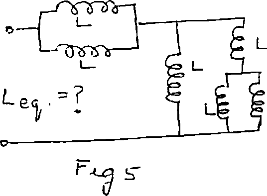
L vwvr<rznm| | r"i 6 UNIT 11 l <5*0 (a) Draw the block diagram of op-amp showing the four major stages. Explain the function of each stage. (b) Explain why an op-amp is desired to haw a high input resistance and low output 2 5 resistance. (c) Discuss the working of inverting and non-iiverting summing amplifiers. (a) Why is it desirable for an op-amp to have a high CMRR? (b) For an ideal op-amp, the differential g,in Ad and CMRR are 106 and 80dB respectively. Calculate the total output voltage if voltages applied at the input are V. = -0.05mV & V. = -0.08mV. (c) Derive an expression for closed loop gain of an inverting amplifier. Calculate the required values of external resistors Ri and Rf- if the circuit is desired to have a gain of 20. UNIT III (a) Draw' the logic circuit and timing waveform for a Mod-5 up counter. Each FF has a rrnnng.nfion delay from clock to O of 1 Or.0. For the counter to cycle from 001 to Oil, how much time is taken? ---- (b) Minimize the expression: f =. A G G -h A S (c) Implement the Boolean function f, using NOR gates only: 5 - A + c d (a) Draw the output waveform of the logic circuit as shown in fig.8 for the input waveforms shown in fig.9. (b) Discuss the race around condition in JK flip-flop. How is it eliminated using master-slave JK flip-flop? (c) Simplify: f = ( ( A+ fi-c ; -t- D ( E+ F )) 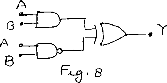  t a F.q -------------the end-
You are here:
PAPER
| |||||||||||