Centre for Development of Advanced Computing(C-DAC) 2005 M.C.A Computer Aplications -103 - Digital Electronics - - - Question Paper
(Please Write your Exam Roll No. immediately) Roll No.
|
FIRST SEMESTER [MCA] - DECEMBER 2005 | ||||||
| ||||||
|
Q. 1. (a) Explain AND, OR and NOT gate using diodes and transistor circuit. | ||||||
(b) Find the 16 complement of AF3B
(c) Convert AF3B to binary.
(d) What is the largest binary number that can be expressed with 12 bits? What is the equivalent decimal and hexadecimal?
(e) What is the exact number 6-bytes in a system that contain.
(i) 32K Bytes
(ii) 64 M Bytes
(iii) 6.4 G Bytes
Q. 2. (a) Simplify the following Boolean function using five variable mps.
F(A, B, C, D, E) = (0, 1, 4, 5, 16, 17, 21, 25, 29)
(b) Simplify the following Boolean function in the product of sums :-F (W, X, Y, Z) = (0, 2, 5, 6, 8, 10)
Q. 3. (a) Design a 4-bit gray code to binary code converter.
(b) Design a 4-bit circuit incrementer using four half adder.
Q. 4. (a) Construct a 4-to-16-line decoder with five 2-to-4-line decoder with enable.
(b) Design a BCD adder subtractor circuit.
Q. 5. (a) Design a 3-bit synchronous counter using D flip-flop.
(b) Design a serial 2s complementer with a shaft register and a flip-flop. The binary number is shifter out from one side and its 2s complement shifted into the other side of the shift register.
Q. 6. (a) Explain internal diagram of OP-Amp.
(b) Draw the architecture of 8085 microprocessor.
(b) Explain successive approximation ADC.
Q. 8. Write short note (any two) :-
(a) PLD
(b) PAI
(c) CAM
(Please Write your Exam Roll No. immediately) Roll No.......
|
FIRST SEMESTER [MCA] - DECEMBER 2004 | ||||||
| ||||||
|
Q. 1. (a) Reduce the following:- | ||||||
(i) AB + A + AB
(ii) (AB + C) (AC + BC) + ABC + AB
(b) Give the block diagram of exclusive OR (XOR) gate using 4 NAND gates only. Write its truth table also.
(c) Subtract (01001)2 from (01000)2 using
(i) 1s Complement method.
(ii) 2s Complement method.
(d) What is the range of signed and unsigned decimal values that can be represented by 8-bits?
Q. 2. (a) Perform the BCD addition of numbers 286 and 548.
(b) Design a Gray to Binary code converter using NAND gates only.
F (W, X, Y, Z) = X (0, 2, 5, 6, 8, 10)
(c) Convert the decimal number 3567 to
(i) Hexadecimal Number
(ii) Octal Number
Q. 3. (a) Show how the following expression can be implemented using NAND gates only.
X= (A+B) (C+D)
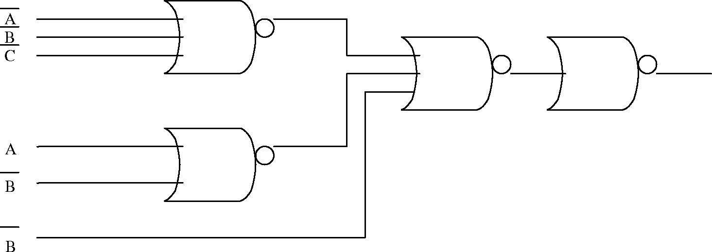
(b) For the following circuit, determine the Boolean function for the output F. Also obtain an equivalent circuit with fever NOR gates.
 |
F |
Q. 4. (a) Minimize the four variable logic function.
f(A, B, C, D) = (A + B +"C + D) (A + C + D).(A + B + C + D).
(B + C) .(B + C).(A +~B).(B + D)
(b) Implement the expression using 8:1 multiplexer f (A, B, C, D) = t m(0, 2, 3, 6, 8, 9, 11, 14)
Q. 5. (a) What do you understand by race around condition in a J-K flip flop? How is it removed in J-K master Slave flip-flop? Explain the working of master-slave flip-flop in detail by giving its block diagram and truth table.
(b) Design a J-K type synchronous counter to count the following states.
5, 8, 2, 7, 13, 0, 5,...........
Q. 6. (a) Explain the working of an 8-bit serial-in-parallel-out shift register by
giving its block diagram. How long will an 8 bit binary number take in this register if the lock frequency is
(i) 1 Mhz
(ii) 5 Mhz.
(b) Explain the working of an OP-AMP based Schmitt Trigger Circuit.
Q. 7. (a) Explain the ladder method of a D/A converter. How does this method overcome the disadvantages of a weighted register method?
(b) Show how to expand 256 x 4 RAMs to obtain a memory expansion of 1024 x 4.
Q. 8. (a) Give and explain the concept of a tri-state buffer circuit. Write its advantages also
(b) What is a microprocessor? Give the pin diagram of an 8085 p and briefly explain the pin architecture. Give your answer with reference to the system bus architecture and register organization of 8085 p.
|
FIRST SEMESTER [MCA] - DECEMBER 2002 | ||||||
| ||||||
Q. 1. (a) Convert the following numbers into decimal: (10110.0101)2 , (16.5)16 and (26.24)8 (1.11010)2 , (132)8 , (5A9)16
(b) The state of a 12-Bit register is 100010010111. What is its content if it represents.
(i) Three decimal digits in BCD.
(ii) Three decimal digits in the excess-3 code.
(iii) Three decimal digits in the 8421 code.
Q. 2. (a) Explain the function of Bipolar junction transistor. Differentiate between BJT and Schottky Transistor.
(b) Explain field effect transistor. Differentiate between FET and BJT.
Q. 3. (a) Simplify the following Boolean function in
(i) Sum of product and
(ii) Product of Sums
F(A, B, C, D)= X(0, 1, 2, 5, 8, 9, 10)
(b) Design a 31 x 1 multiplexer using two 16 x 1 multiplexer and one OR gate.
Q. 4. (a) Design a 3-bit Binary to Gray code and Gray to Binary code converter.
(b) Design a 4-bit Adder with carry look ahead generator.
Q. 5. (a) Design a 3-bit counter using T-flip flop (b) Design a 4-Bit Right Shift Register.
Q. 6. (a) Find the output waveform of an OP Amp under the following conditions.
(i) Inverted input terminal connected to ground and a sinusoidal signal of 4v peak at the non-inverting input.
(ii) Non-inverting input terminal connected to ground and a sinusoidal signal of 4v peak at the inverting input.
(b) Design a square wave generator using Schmitt trigger and draw a waveform. Explain in detail.
Q. 7. (a) Explain functional Block diagram of 8085 microprocessor.
(b) What is Analog to digital converter? How many types of ADC can be designed? Explain any one ADC design technique.
Q. 8. Write short note
(a) CCD
(b) Content Addressable Memory.
|
FIRST SEMESTER [MCA] - DECEMBER 2001 | ||||||
| ||||||
Q. 1. (a) Perform the conversions:
(i) (.6875)10 to octal.
(ii) (250)io to base 4.
(b) (i) Convert 11010111.110 to hexadecimal
(ii) Convert 2AC5.D to decimal.
(c) Perform subtraction using 2s complement and 1s complement 10010 - 10011
Check the result by straight subtraction.
(d) (i) Name any one reflected code and one weighted code.
(ii) What do you mean by parity? How is a parity bit used in error detection?
Q. 2. (a) Define the following terms
(i) FET
(ii) CMOS
(b) Simplify using K-maps and realize using NAND gates F=m (0, 1, 2, 3, 11, 12, 14, 15)
(c) Design a 4-bit ADDER / SUBTRACTOR circuit with ADD / SUB line.
Q. 3. (a) Explain parity generator / checker. Give block diagram of a 9-bit odd parity checker using single 74180 and an inverter.
(b) Name the various flags in 8086 microprocessor
(c) Briefly explain any 4 characteristics of digital ICs
Q. 4. (a) Design a synchronous decade counter. Describe what do you understand by lock up condition.
(b) Explain the working of a shift register with the help of an example.
Q. 5. (a) What are A/D and D/A converters? Explain any one of the two with an example.
(b) Briefly explain the following
(i) PLD
(ii) Instruction set of a microprocessor.
Q. 6. (a) Discuss various types of ROMs
(b) Write short note on CAM.
(c) Explain with diagram the working of a bipolar RAM cell.
Q. 7. (a) What is race around condition? How is this solved in flip-flops?
(b) What are parity encoders Q. 8. (a) Explain various arithmetic instructions of 8085 microprocessor.
(b) Briefly explain the interrupt system of 8085.
(c) What are the major drawbacks of using high level languages?
|
FIRST SEMESTER [MCA] - DECEMBER 2001 | ||||||
| ||||||
Q. 1. (a) Simplify the following Boolean functions 3
(i) F (A, B, C) = (0, 2, 4, 5, 6)
(ii) F (w, x, y, z) = (0, 2, 8, 9, 10, 11, 14, 15)
(b) What is Dont Care condition. 2
(c) Differentiate between:- 4
(i) Combinational and sequential circuit
(ii) Static and Dynamic RAM
(iii) Volatile and Non-Volatile memory.
(d) Explain the following terms:- 6 (i) Latch (ii) Trigger
(iii) Ex-OR gate (iv) Complement Number
(v) State Table (vi) Register
(e) Show that a JK Flip-flop can be converted into a D Flip-flop with an inverter between J & K inputs. 4
(f) Convert following number as directed:- 3
(i) 0.375 Decimal to Binary
(ii) 5A9 Hexadecimal to decimal
(iii) 2747 Decimal to Octal
(iv) 132 Octal to Binary
(g) Write short notes on Any four:- 8
(i) Multiplexer (ii) TTL
(iii) R-S flip flop (iv) Binary Counter
(v) CCD (vi) Tunnel Diode
Q. 2. (a) Design a full subtractor using NAND and NOR gates. 4
(b) Describe CMOS logic circuit using a two input AND gate circuit. 3.5
(b) Give various I/O and Interfacing devices used with 8085 along with their functions and chip numbers. 4
Q. 4. (a) Design a 4 x 1 multiplexer. 4
(b) Give a functional diagram for 4-bit register with parallel load. 3.5
Q. 5. (a) Show the circuit of a 5 x 32 decoder constructed with four 3x8 decoder
(with enabled inputs) and one 2 x 4 decoder. 4
(b) How does a content addressable memory work? 3.5
Q. 6. (a) What is A/D converter? Explain its working. Give its applications. 4
(b) What is PLA? Implement following function using PLA 3.5
Z = x * y + y * w
Q. 7. (a) What is De-Morgans Law? Show that any sum of product circuit can be converted into product of sum circuit using an example. 3.5
(b) Design an 8-bit ripple counter. 4
Q. 8. (a) Explain the working of Master slave flip flop. 3.5
(b) Design a 4-bit left shift register. 4
Q. 9. (a) Give a functional diagram of ALU. 3.5
(b) Design a Seven Segment Display circuit. 4
FIRST SEMESTER [MCA] - DECEMBER 2001 Paper Code: MCA-103 Subject: Digital System
Time: 3 Hours Maximum Marks: 60
Q. 1. Do as directed (Any 6)
(a) Convert the following decimal nos. equivalent hexadecimal (do not convert decimal to binary first and then to hexadecimal). Show the steps.
(i) 262 (ii) 397
(b) Convert the following decimal nos. into binary nps. using 9s and 10s complement.
(i) 2122 (ii) 37.623
(c) Perform the following subtraction using 2s complement. Indicate the sign of the result
(i) 1010 - 1011 (ii) 01100 - 00011
(d) How can you connect NAND to get the following.
(i) AND Gate (ii) OR Gate
(e) Draw a logic circuit for F = AlC + ABC
Next simplify the equation with Boolean algebra and draw the simplified logic circuit.
(f) Realize the following: using 8:1 multiplexer F = Xm (0, 3, 5, 6, 9, 10, 12, 15)
(g) Define the following
(i) Digital Comparator
(ii) Bi-polar Junction Transistor
Q. 2. Answer the following
(i) Minimize the following function F = Xm (0, 3, 5, 6, 9, 10, 12, 15)
(ii) Explain the operation of 4-bit bi-directional shift register.
(iii) Convert the following to POS form.
AB + A (B + C) (D + B)
Q. 3. Write short notes
(a) Full Subtractor
(b) ALU (74181)
(c) Master-Slave Flip-flop
Q. 4. (a) Design a counter with the following specifications
(i) The counter is to work in mod-5 when control input is 0.
(ii) The counter is to work in mod-8 mode when control input is 1.
(b) Define the following
(i) set-up time (tsetup) (ii) hold time(thold)
Q. 5. (a) A J-K flip flop is to be used to get a T flip flop.
(b) Explain the race around condition in J-K flip flop.
Q. 6. Describe in detail the working of 8086 up giving the entire register set and
other components. Explain the working of BIU and EU hoe the 16 bit offset in 8086 are converted to 20 bit addresses.
Q. 7. (a) Design a circuit to follow the given sequence T flip flop 0-1-2-4-6
(b) Explain the working of Monostable multi-vibrator.
Q. 8. Describe the following
(a) PLAs
(b) Parity Generator
(c) High level language
(d) Logical instruction of 8085
(e) Types of ROM
Q. 9. (a) Show that (NAND) is functionally a complete set of gates.
(b) What is RAM? Describe the different types of RAM.
(c) What is meant by Direct and Indirect addressing in 8085. Explain with examples.
|
Attachment: |
| Earning: Approval pending. |