West Bengal Institute of Technology (WBIT) 2008-5th Sem B.Tech Electronics and Communications Engineering Electronics & Comm ( - ) Microoprocessor & Microcontroller - Question Paper
CS/B.Tech(ECE)/SEM-5/EI(EC)-502/08/(09) o

ENGINEERING & MANAGEMENT EXAMINATIONS, DECEMBER - 2006
MICROPROCESSOR & MICROCONTROLLER
Time : 3 Hours ] [ Full Marks : 70
GROUP - A ( Multiple Choice Type Questions )
1. Choose the correct alternatives for any ten of the following : 10 x 1 = 10
i) The control signal used to distinguish between an I/O operation and memory operation is
a) ALE b) IO/M
c) SID d) SOD.
ii) The control signal, HOLD is sent by 8085 in order to
a) inform I/O device that the address is being sent over the AD line
b) achieve separation of address from data
c) synchronize with low speed peripheral
d) to activate DMA.
iii) The number of bytes of RAM contained in 8155 is
a) 256 b) 512
c) 1024 d) 2K.
iv) In "JZ NEXT" instruction of 8051 microcontroller which register's content is checked to see if it is zero ?
a) A b) B
c) Rl d) R2.

v) If ready pin is grounded, it will introduce.....................states into the bus cycle
of 8086/8088 microprocessor.
a] wait b) idle
c) wait and remains idle d) all of these. _
vi) Whenever the POP H instruction is executed
a) data bytes in the HL pair are stored on the stack
b) two data bytes at the top of the stack are transferred to the HL reg. Pair
c) two data bytes at the top of the stack are transferred to the PC
d) two data bytes from the HL register that were previously stored on the
stack are transferred back to the HL registers,
vii) For 8255 PPI, the bidirectional mode of operation is supported in
a) mode 1 b) mode 2
c) mode 0 d) either (a) or (b).
viii) If a DMA request is sent to the microprocessor with a high signal to the HOLD pin, the microprocessor acknowledge the request
a) after completing the present cycle
b) immediately after receiving the signal
c) after completing the program
d) none of these.

ix) STA 9000H is a
a) data transfer instruction
b) logical instruction
c) I/O and machine control instruction
d) none of these.
x) The segment and off-set address of the instruction to be executed by 8086 microprocessor are pointed by
a) CS and SI
DS and IP
b)
c) CS and SP
d)
CS and IP.
b) instruction address
none of these.
d)
xi) The instruction register holds
a) flag conditions c) opcodes
xii) The instruction SHLD
a) stores the values of H-L pair to a specified memory location
b) stores the values from specified memory location to H-L pair
c) stores the values of H-L pair to accumulator
d) none of these.
GROUP - B ( Short Answer Type Questions )
3 x 5 = 15
Answer any three of the following.
What is the difference between a Latch and a Buffer ? Explain why a latch is used for an output port, but a tri-state buffer can be used for an input port. 5
bnriUhd I
3. The following sequence of instructions are executed by an 8085 microprocessor :
C000 LXI SP, D7FF
C003 CALL C008 C008 POP H
What are the contents of the stack pointer ( SP ) and HL register pair on completion of execution of above instructions ? 5
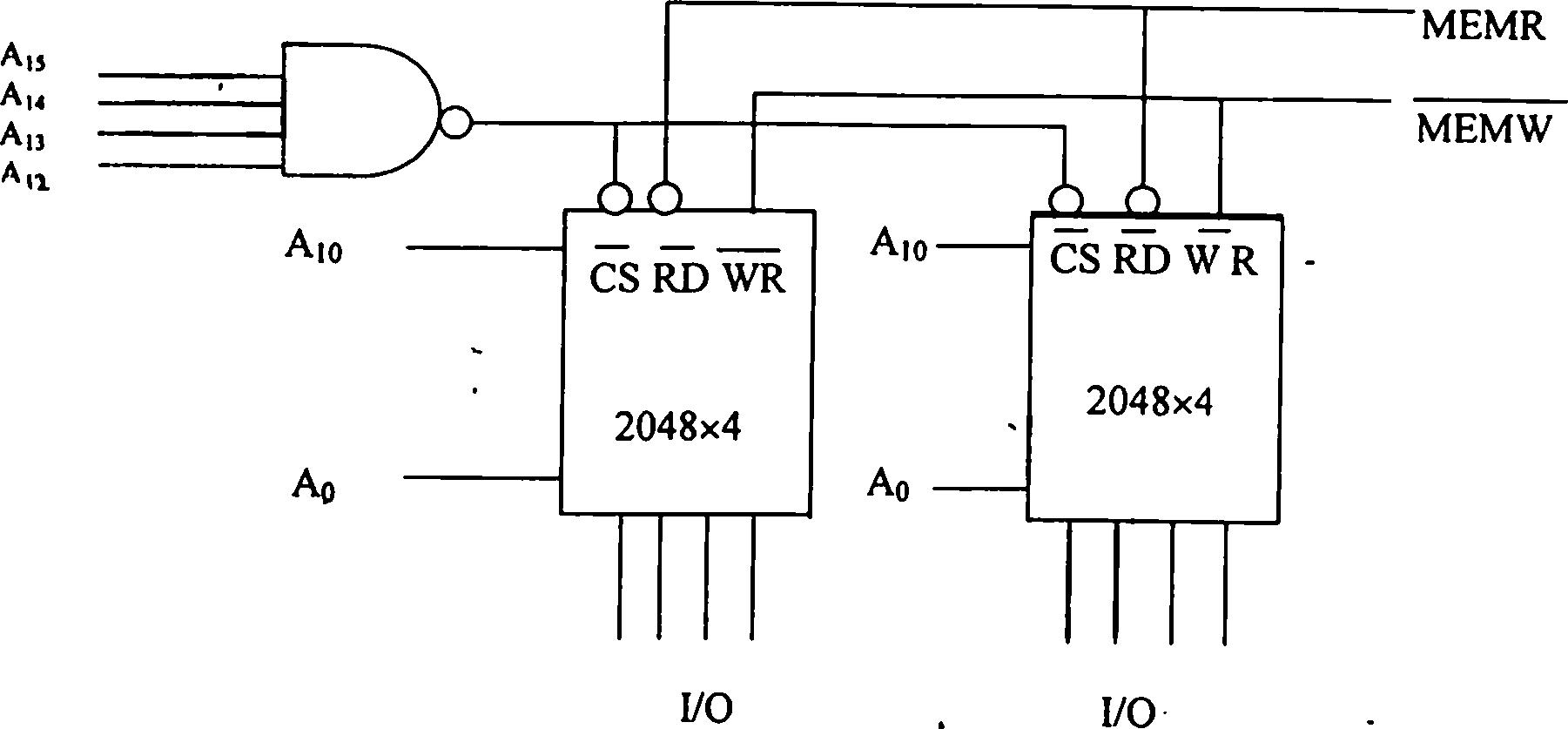
4. Specify the entire memory map of the schematic shown in the figure and explain the significance of the don't care address line on memory address. 5
5. a) Explain the function of the following pins of 8085 :
READY. INTR. 2
b) Discuss the functions of the following instructions of 8085 :
ADC H. LHLD 8000. 3
6. What are interrupts ? How many interrupts are there ? What are mask able and nonmask able interrupt ? Discuss SIM instruction. 5

GROUP - C ( Long Answer Type Questions )
Answer any three of the following. 3 x 15 = 45
7. a) Write an 8085 ALP for 1 ms delay. Assume the system elk period as 0-33 p sec.
Calculate the maximum delay for that subroutine.
b) What is the use of HOLD and HLDA pin of 8085 pp ?
c) What are the addressing modes of the following instruction ?
i) LDAX D
ii) XTHL
iii) SHLD 20FFH
iv) LXI B. 108AH
d) Explain the function of ADC B and STA 9000H. 5 + 4 + 4 + 2
8. a) What do you mean by addressing mode ? What are the different addressing
modes supported by 8086 ? Explain each of them with suitable examples.
b) What is the difference between the physical address and the logical address ?
c) How many flags are there in 8086 microprocessor and what are they ?
d) Explain the burst mode data transfer and cycle stealing in context of DMA data transfer scheme. (1 + 5)'+ 2 + 2 +5
9. a) What are the main functions of BIU and EU unit in 8086 microprocessor ?
b) Draw the block diagram of 8254 timer and describe briefly its different sections.
c) What are two key lockout and N-key roller mode in 8279 ?
d) Explain interrupts in 8051 microcontroller. (2 + 2J + 5 + 3 + 3
10. a) Draw the timing diagram for LEJA instruction.
b) What do you mean by MODE 0, MODE MODE 2 operation of 8255 ?
c) Write the BSR control word for setting PC4 in 8255 A.
d) What are the functions of major components in 8259 interrupt controller ?
e) What is polling in 8259 ? 5 + 4 + 2+ 2 + 2
11. a) Draw the timing diagram of the instruction OUT 08H stored from memory
location 8000H.
b) Write a program in assembly language for 8085 pP to periodically turn on and off two switches by setting up 8255 PPI to BSR mode. The duty cycle is 50%.
c) An 8 bit binary number ( e.g., 9FH ) is stored in memory location 8050H.
i) Write a program in assembly language for 8085 pP to w) transfer the byte to the accumulator.
x) separate the two nibbles ( as 09 and 0FH ).
y) call the subroutine to convert each nibble into ASCII Hex Code.
z) store the codes in memory locations 8060 and 8061H.
ii) Write a subroutine to convert a binary digit ( 0 to F ) into ASCII Hex Code.
5 + 4 + 6
END
55004 ( 5/12 )
|
Attachment: |
| Earning: Approval pending. |