Vellore Institute of Technology 2008 M.Tech VLSI system design Analysis & Design of Digital Integrated Circuits - Question Paper

![]() VIT
VIT
U N I V E R S I T Y
(Estd. u/s 3 of UGC Act 1956)
School of Electrical Sciences
Discipline: M.Tech(VLSI Design) Semester:I
Subject: analysis and design of Digital Integrated Circuits Exam: CAT-I
Full Marks:50 Time: 1-1/2 hrs
Instructions: Answer ALL questions
![]()
1. For the circuit in Figure, Vs = 3.3 V. Assume AD = 12 μm2, φ0 = 0.65 V, (10)
and m = 0.5. NA = 2.5 E16 and ND = 5 E15.
a) Find ID and VD.
b) Is the diode forward- or reverse-biased?
c) Find the depletion region width, Wj, of the diode.
d) Use the parallel-plate model to find the junction capacitance, Cj.
e) Set Vs = 1.5 V. Again using the parallel-plate model, explain qualitatively why Cj
increases.
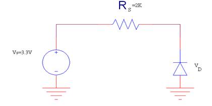 fig:1
fig:1
2. Consider a CMOS inverter with the following parameters (8)
nMOS: VTn=0.6V, μnCox = 60μA/V2 , (W/L)n = 8
pMOS: VTp = -0.7V, μpCox = 25μA/V2 , (W/L)p = 12
calculate the noise margin and the switching threshold(VTH) of the circuit. The power supply voltage is VDD = 3.3V.
3.
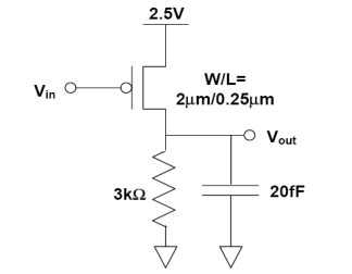 fig:2
fig:2
Assume the switch model behavior of PMOS transistor. When Vin> 1.25V, resistance of the transistor is infinite and when the Vin< 1.25V, the transistor can be modeled as having a resistance of 50Ω. (a) Determine the VOH and VOL. Explain the answer, (b) Calculate the tPLH and tPHL to obtain the average of propagation delay tp. (10)
4. A two-stage buffer is used to drive a metal wire of 1 cm. The first inverter is of minimum size with an input capacitance Ci=10 fF and an internal propagation delay tp0=50 ps and load dependent delay of 5ps/fF. The width of the metal wire is 3.6 μm. The sheet resistance of the metal is 0.08 Ω/ , the capacitance value is 0.03 fF/μm2 and the fringing field capacitance is 0.04fF/μm.
a) What is the propagation delay of the metal wire?
b) Compute the optimal size of the second inverter. What is the minimum delay through the buffer?
c) If the input to the first inverter has 25% chance of making a 0-to-1 transition, and the
whole chip is running at 20MHz with a 2.5 supply voltage, then whats the power consumed by the metal wire? (10)
5.
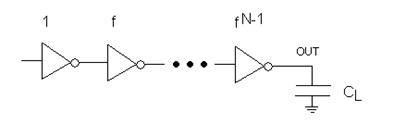 fig: 4
a) What is the delay of a minimum sized inverter driving another inverter f times its size? For the minimum sized inverter, assume input capacitance equal to 3Cunit, equivalent resistance through the NMOS or PMOS equal to Runit, and intrinsic (self-loading) capacitance on the output also equal to 3Cunit. Assume that the capacitance and resistance values scale linearly with size. Your answer will be in terms of these parameters (no calculations!). Take the limit as f goes to 0 and call the result inv.
b) How much energy is consumed by the driving inverter after successive low to high (L→H) and high to low (H→L) transitions, in terms of a supply voltage Vdd?
c) Consider the chain of N progressively sized inverters shown in Figure 2 (the first is minimum sized). If the output load CL=96 Cunit, what sizing factor f would minimize the total delay for a chain of N=5 inverters? Find the total delay of this chain in terms of inv.
d) Find the optimum number of inverters and sizing ratio for the output load specified in Part (c). Express the optimum delay again in terms of inv. Considering your result for Part (b), do you think this inverter chain will consume more or less energy than a single inverter driving the output load? (12)
| Earning: Approval pending. |