Osmania University (OU) 2006-1st Sem B.E Electronics & Tele-Communication Engineering 3/4 (E.C.E)(ESTER)SUPPLEMENTARY ,IL, Linear integrated circuits and applications - Question Paper
B.E 3/4 (E.C.E)(I-SEMESTER)SUPPLEMENTARY EXAMINATION,APRIL,2006
Linear integrated circuits and applications
Code No.: 10293
FACULTY OF ENGINEERING B.E. m/IV Yer (ECE) I Semester (Supplementary) Examination, May 2006
LINEAR INTEGRATED CIRCUITS AND APPUCATIONS Time : 3 HoursJ [Max, Marks : 75
Answer all questions of Part A.
Answer five questions from Part B.
Part A - (Marks : 25)
1. List the Op Amp parameters that are important for ac applications. What are their : practical significance.
2. Obtain the output expression for the following circuit
|
R |
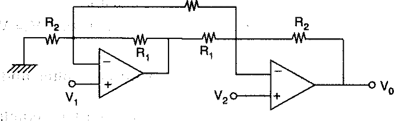 |
3.;; jiWhat is all pass filter? Where and why is it needed?
4. .What are thq vantages of active filters over passive ones.
5. State the relationship between lock range and capture range through a mathematical
1 expression and explain.
(b) Define input offset and output offset voltage of an Op Amp. Draw the differential amplifier with offset voltage compensating network and explain its operation.
12. (a) Draw the frequency response curve of a differentiator. How is it modified when
11. (a) In the circuit shown below calculate the ampHtxide of ebito voyage
Vcm. If the induced 60Hz noise at the output is 5V(rms).
4.7K
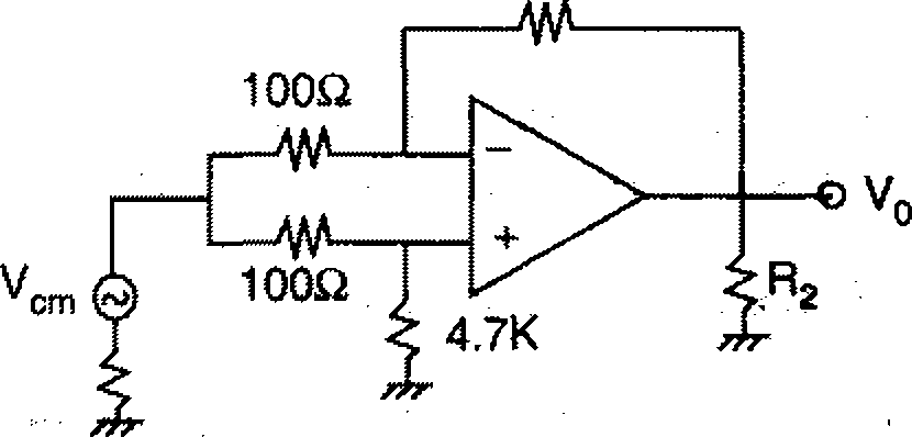
a small resistor is connected in series with the capacitor.
(b) Design a difference amplifier (using one Op Amp). Such that VQ= V2~3Vj and Ri j = Ri2 = 100 K.
13. (a) Draw the circuit of a second order narrow band-pass filter and derive an
expression for its transfer function.
(b) Design a fourth order butterworth high pass active filter for a cutoff frequency of 2.5 kHz with a pass-band gain of 6.
14. (a) Draw the circuit of a Schmitt trigger which is required to cocfipiare the input
signal against the fixed reference of +2V. The output is to switch states whenever input goes below or above 2V by 0.5 mV. The input source is 50&. Current Ib = 0.5|iV. Common mode input (max) is 5V. Assume offset is O.
(b) Draw the internal functional diagram of IC 555 and explain the fur}Ct|Qp$ of each. P in.
15. (a) Design the circuit of IC 7805 voltage regulator for 5V at 1.5 Amp load current. 4
(b) Draw the circuit of a IC 723 voltage regulator for 6V at: 200ma. Explain the current fold back feature of this IC voltage regulator. 6
|
Attachment: |
| Earning: Approval pending. |