Osmania University (OU) 2006-2nd Sem B.E Electronics & Tele-Communication Engineering 2/4 (E.C.E)(ESTER)SUPPLEMENTARY ,IL, Analog electronic circuits - Question Paper
B.E 2/4 (E.C.E)(II-SEMESTER)SUPPLEMENTARY EXAMINATION,APRIL,2006
Analog electronic circuits
Code No.: 10046
FACULTY OF ENGINEERING B.E. II/IV Year (ECE) II Semester (Main) Examination, April 2006
ANALOG ELECTRONIC CIRCUITS Time : 3 Hours] [Max. Marks : 75
Answer all questions of Part A.
Answer five questions from Part B.
Assume any data if missing.
Part A - {Marks : 25)
1. Sketch the frequency response of a transformer coupled amplifiers. Give the reasons for the fall in gain at low and high frequencies. 3
2. What is the range of frequency in terms of *fT upto which the hybrid-rc equivalent circuit of CE amplifier is valid? 2
3. What is harmonic distortion in power amplifiers and why does it occur? 2
4. Why class AB is preferred over class B in audio frequency power amplifiers. 2
5. An amplifier has an open loop voltage gain 1000 100. If 10% negative feedback is introduced, what will be its closed loop voltage gain and its variation? 3
6. Comment why RC oscillators cannot be used at radio frequencies, 2
7. What factors decide the frequency stability of an oscillator? 3
8. Sketch the frequency response of a staggered tuned amplifier. State its advantages over cascaded single tuned amplifiers. 3
9. State the advantages of class C power amplifiers over class B tuned power amplifiers.2
10. What are the limitations of zener voltage regulators and how do you over-come them? 3
I. (a) Explain the role of emitter by pass capacitance on the low frequency response of an RC coupled CE amplifier. 4
(b) A BJT is tuned to have fT= 500 MHz, = 100 mmhos, hfc = 100 and Cbc 5pF. It is used as an CE amplifier with Rs = 1 Si and = 2K2. Assume rbb = 0. Determine for the amplifier (i) the mid-band voltage gain (vQ/vs) and (ii) upper 3-dB cutoff frequency. 6
(a) What is cross over distortion in class B push pull amplifier and how do you eliminate it? Explain your answer with a neat circuit diagram and waveforms. 4
(b) A power transistor is used as a class A transformer coupled amplifier and is to deliver a maximum of 5 watts to a 4 ohm load. Operating point is adjusted for symmetrical clipping with collector supply voltage of 20V. Assume ideal characteristics with Vm<Ti = 0. Calculate for the amplifier (i) Transformer turns ratio (ii) peak collector current and (iii) collector circuit efficiency, 6
. (a) Prove that negative feedback in amplifiers reduces the distortion. State the assumptions made in your derivation. 4
(b) Design a colpitts oscillator to oscillate at 1 MHz using a BJT having hle = 2 K and hfc = 100. Use capacitances of 1000 pF and 500 pF. Show the circuit diagram with all the component values along with biasing circuit. Derive the expressions used in your design. 6
. (a) What is the possibility of oscillations in a tuned amplifier? How do you neutralize a BJT tuned amplifier against oscillations. Explain your answer with a neat circuit diagram and derive the expressions for the neutralizing components. 5
(b) Draw the circuit diagram of a double tuned transformer coupled voltage amplifier using a BJT. Derive the expressions for its voltage gain at the centre frequency and band-width for critical coupling. 5
(a) State the advantages of SMPS over conventional voltage regulator. Show the block schematic diagram of a SMPS and explain its operation. 5
(b) An unregulated D.C. source of (12 2) V is available and is to be regulated using a zener diode to provide 6 V at 25 mA. A 6 V zener diode is available. Show the circuit diagram with the component values. What is its output impedance? 5
>. (a) A BJT has h. = 2 KQ, h - 10-5, h, = 100 and h. = 25 (iA/V. It is used as an
1C * C !6 OC
emitter follower amplifier with Rs = 1KX2 and RL = 5KL Determine for the amplifier
Avs * vo/vs, R1 and R. 5
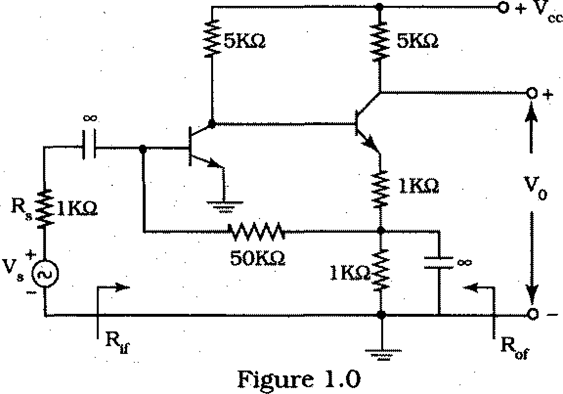
(b) For the two stage feedback amplifier shown in figure 1.0, determine the voltage gain A = vo/vs, and Rof Assume that the transistors are identical and have hle = 2KQ, hfe = 80 as parameters. 5
7. (a) What is a flyback converter? What are its advantages? Show the circuit diagram of a voltage regulator with fly back and explain its operation. 4
(b) Draw the circuit diagram of a tuned class C power amplifier and explain its operation with waveforms. Give the complete analysis of the amplifier and derive the expression for its output power and collector circuit efficiency. 6
|
Attachment: |
| Earning: Approval pending. |