Visvesvaraya Technological University (VTU) 2005 B.E Basic Electronics - Question Paper
First Semester B.E Degree Examination, July/August 2005
Common to all Branches
Basic Electronics
Full ques. Paper in attachment
Page No... 1 ELN15/25
|
\m |
s |
0 |
lA |
c |
s |
o |
i |
6 |
USN First/Second Semester B.E Degree Examination, July/August 2005
Common to All Branches
Time: 3 hrs.] {Max.Marks : 100
Note: l. Answer any FIVE full questions.
2. All questions carry equal marks.
1. (a) Explain the mechanism of conduction in P and N type semi conductions using
energy band diagrams. (s Marks)
(b) With the help of diode equation, explain the VI characteristics of a PN junction,
(8 Marks)
(c) The saturation current density of a PN junction Ge diode is 250mA/m2 at 300,l7T. Find the voltage that must be applied across function to cause a forward current density of 105Amp/m2 to How. (4 Marks)
2. (a) Distinguish clearly between Ovalanche breakdown and Zener break down.
(5 Marks)
(b) In a Zoner diode regulator, the input DC is 10V 20%. The output requirement
* are 5V and 20mA. Assuming /3 iriin & If max as 5mA & 80mA. design the zoner diode regulator. _
I
V.
S~V
V<G< Q.Q-C>
(7 Marks)
(c) A full base rectifier has a load of 2kfi. The AC voltage applied to the diodes is 200 - 0 - 200V
* Assuming ideal diodes, calculate i) average DC current ii) average DC voltage & iii) Ripple voltage. If a capacitor of value 500(iF is connected across the load, what is the new value of tUe ripple voltage. Assume / = 50Hz. (8 Marks)
3. (a) Draw the sketch of the output characteristics of a transistor in common emitter configuration ? indicate the various regioij of operation and occount for the shape of characteristics qualitatively. (7 Marks)
(b) Discuss the causes of unstabilitv in a transistor. (6 Marks)
(c) For the circuit shown below a silicon transistor with = 100 is used. Find Ir and VCE- Draw the DC load line on the output characterisi ics and indicate "Q" point. Assume VBE = 0 .7volt j~---J (7 Marks)
+
|
-- | |
|
L- _______________ |
- |
4. (a) What are the causes of distorsion in amplifiers ? Discuss the various types of
distorsion in amplifiers ? How can they be minimized? (s Marks)
(b) Explain the heed for coupling in amplifier ? Mention the different type of
coapling in amplifiers. (4 Mark)
.' * '
(c) With a neat diagram, explain the operation of an RC phase shift oscillator. Indicate Trans Bark bausen*s criterion is satisfied in this case ? (s Marks)
5. [a) Define and mention the importance of the following terms w.r.t an Op. amp -
i) CMRR ii) SCEW base iii) PSRR iv) I/P offset voltage (io Marks)
(b) Show that the op-amp circuit shown below can work as a subtractor.
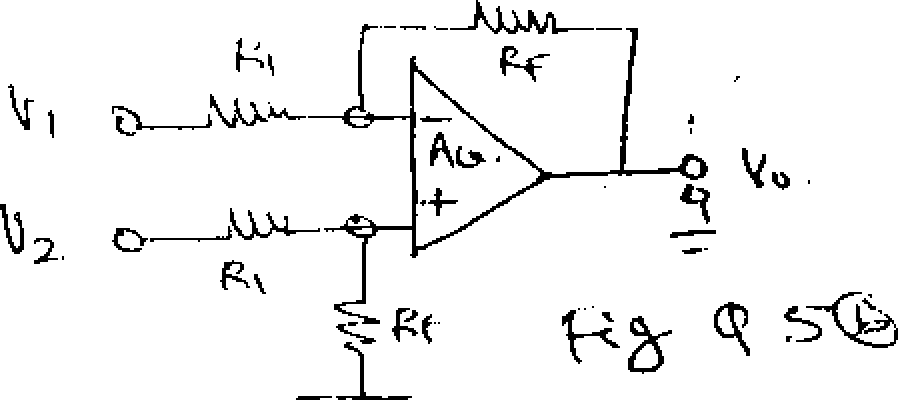
(S Marks)
(c) Design an adder circuit using an op ramp, to obtain an output expression Vo = 2(0. IVj + 05F2 + 20V3) where \\, Vj>&; V3 are the inputs. (5 Marks)
6. (a) Explain the need for modulation in communication systems. (4 Marks)
(b) Explain the principle of frequency modulation. Draw the frequency spectrum of FM wave. {G Marks)
(c) Draw the block diagram of a super heterodyne receiver and explain the function of each stage with necessary waveform. (io Marks)
7. (a) Convert [2AB 8] = [ ? ]10 = [ ? ]6
[764.352]g = [ ? ]1C = [ ? ]2 (4 Marks)
fb) i) Add the S bit nos. 01101011 & 1011 0110 & show the same number in hexa decimal notation.
ii) Subtract the decimal nos. +28 & -19 using twos compliment method.
(5 Marks)
(c) Realize Ex-OR gate using NOT, OR and AND gates only. (5 Marks)
(d) Simplify the following Boolean expressions and realize using only NAND gates.
i) XYZ+XYZ+YZ+Z
ii) {A + BC) (v4 + B -j- C) (A + .?) (6 Marks)
8. (a) Draw the circuit of a DT Nand gate and explain its working. (7 Marks)
(b) Distinguish clearly between combinational logic circuit and sequential logic circuits. (5 Marks)
(c) Explain the working of a CRT. (8 Marks)
|
Attachment: |
| Earning: Approval pending. |