Jawaharlal Nehru Technological University Anantapur 2008 B.Tech Supplimentary s%2C %2F ELECTRONIC DEVICES AND CIRCUITS - 1 - Question Paper
Code No: 07A1EC06 Set No. 1
I B.Tech Supplimentary Examinations, Aug/Sep 2008 ELECTRONIC DEVICES AND CIRCUITS ( Common to Electronics & Communication Engineering, Computer Science & Engineering, Electronics & Instrumentation Engineering, Bio-Medical Engineering, Information Technology, Electronics & Control Engineering, Computer Science & Systems Engineering, Electronics & Telematics, Electronics & Computer Engineering and Instrumentation & Control
Engineering)
Time: 3 hours Max Marks: 80
Answer any FIVE Questions All Questions carry equal marks
1. Derive the expression for the deflection in a magnetic deflection system. Hence obtain the expression for magnetic deflection sensitivity. [16]
2. (a) Explain the volt ampere characteristics of PN diode.
(b) Explain the temperature dependence of VI characteristics.
[8+8]
3. Determine:
(a) DC output voltage,
(b) PIV,
(c) Rectification effeminacy of the given circuit figure3c.
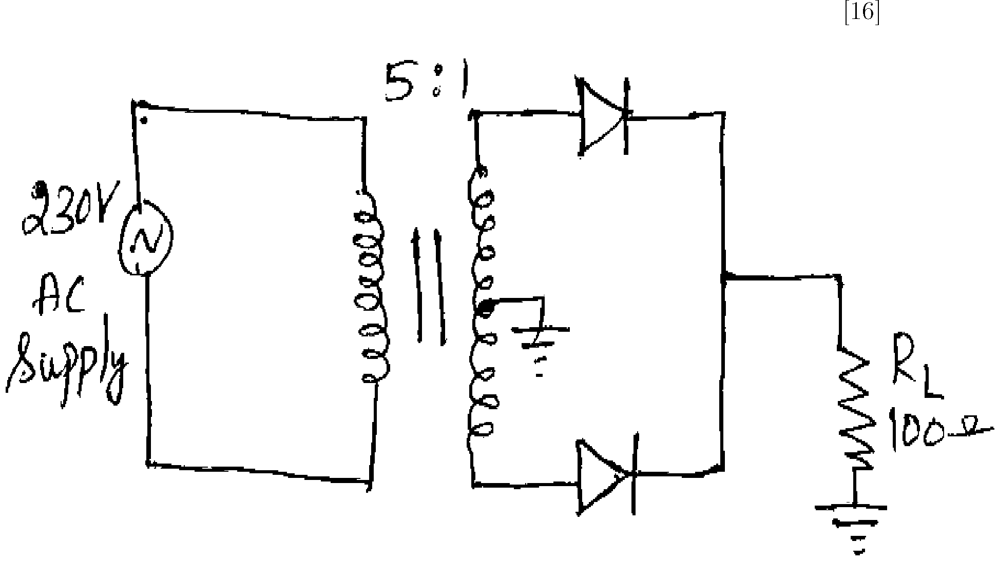 |
|
Figure 3c |
4. (a) Why we call FET as a voltage controlled device?
(b) Write about the broad classification of FET.
(c) Draw the circuit symbol of P Channel N Channel FET.
5. A germanium transistor having fl = 100 and VBE = 0.2 V is used in a fixedbias amplifier circuit where VCC = 16V, Rc = 5 K Q, and RB = 790 kQ. Determine its operating point. [16]
[4+6+6]
6. A transistor used in a CC Circuit as shown in Figure 6. has the following set of h parameters.
hic = 2 KQ, hfc = -51, hrc = 1, hoc = 25 x 10-6
Find the values of input and output resistances, current and voltage gains of the amplifier stage. Use the approximate analysis. [16]
 |
|
Figure 6 |
7. Draw the practical circuit for Current series feedback and find the voltage gain, input impedance & output impedance. [16]
8. Design a phase shift oscillator to operate at a frequency of 2 KHz using a JFET. Assume that = 50 and rd = 5 KQ and the phase shift network does not load the amplifier,
(a) Find the minimum value of RD to be used in the drain circuit.
(b) Find the value of the RC Product.
(c) Choose reasonable values of R and C to make this oscillator work satisfactorily.
[16]
I B.Tech Supplimentary Examinations, Aug/Sep 2008 ELECTRONIC DEVICES AND CIRCUITS ( Common to Electronics & Communication Engineering, Computer Science & Engineering, Electronics & Instrumentation Engineering, Bio-Medical Engineering, Information Technology, Electronics & Control Engineering, Computer Science & Systems Engineering, Electronics & Telematics, Electronics & Computer Engineering and Instrumentation & Control
Engineering)
Time: 3 hours Max Marks: 80
Answer any FIVE Questions All Questions carry equal marks
1. Derive the expression for the deflection in an electrostatic deflection system. Hence obtain the expression for electro static deflection sensitivity. [16]
2. (a) What is diffusion length (L)?
(b) A Diode operating at 300 k at a forward voltage of 0.4V carries a current of 10ma when voltage is changed to 0.42V the current becomes thrice. Calculate the value of reverse leakage current and n for the diode (Assume VT = 26 mv).
[4+12]
3. Derive the ripple factor of n- Filter with neat sketch. [16]
4. Derive an Ebers Moll equation for a transistor. [16]
5. (a) Explain the criteria for fixing operating point.
(b) List out the different types of biasing methods. [12+4]
6. A transistor used in a CC Circuit as shown in Figure 6. has the following set of h parameters.
hic = 2 KQ, hfc = -51, hrc = 1, hoc = 25 x 10-6
Find the values of input and output resistances, current and voltage gains of the amplifier stage. Use the approximate analysis. [16]
 |
|
Figure 6 |
7. Briefly explain the current shunt feedback, also find the gain, input impedance and output impedance. [16]
8. Explain the operation of a transistorized Wein-bridge oscillator with the help of neat circuit diagram. How is amplitude stability achieved in this circuit? [16]
I B.Tech Supplimentary Examinations, Aug/Sep 2008 ELECTRONIC DEVICES AND CIRCUITS ( Common to Electronics & Communication Engineering, Computer Science & Engineering, Electronics & Instrumentation Engineering, Bio-Medical Engineering, Information Technology, Electronics & Control Engineering, Computer Science & Systems Engineering, Electronics & Telematics, Electronics & Computer Engineering and Instrumentation & Control
Engineering)
Time: 3 hours Max Marks: 80
Answer any FIVE Questions All Questions carry equal marks
1. A charged particle having charge thrice that of an electron and mass twice that of an electron is accelerated through a potential difference of 50 V before it enters a uniform magnetic field of flux density of 0.02 Wb/m2 at an angle of 25o with the field. Find [16]
(a) The velocity of the charged particle before entering the field,
(b) Radius of the helical path, and
(c) Time of one revolution.
2. (a) Explain about semiconductor, Insulator & Conductor with neat sketch.
(b) State the Einstein relationship for semiconductor.
(c) State paulis exclusion principle. [6+5+5]
3. (a) Why do we need filters in a power supply under what condition we shall prater
a capacitor filter?
(b) Draw the block diagram of RPS.
(c) What is the function of a bleeder resistor?
(d) Describe the terms capacitor input filter and inductor input filter.[5+2+5+4]
4. With a neat sketch explain the drain source characteristics & transfer characteristics of enhancement type MOSFET. [16]
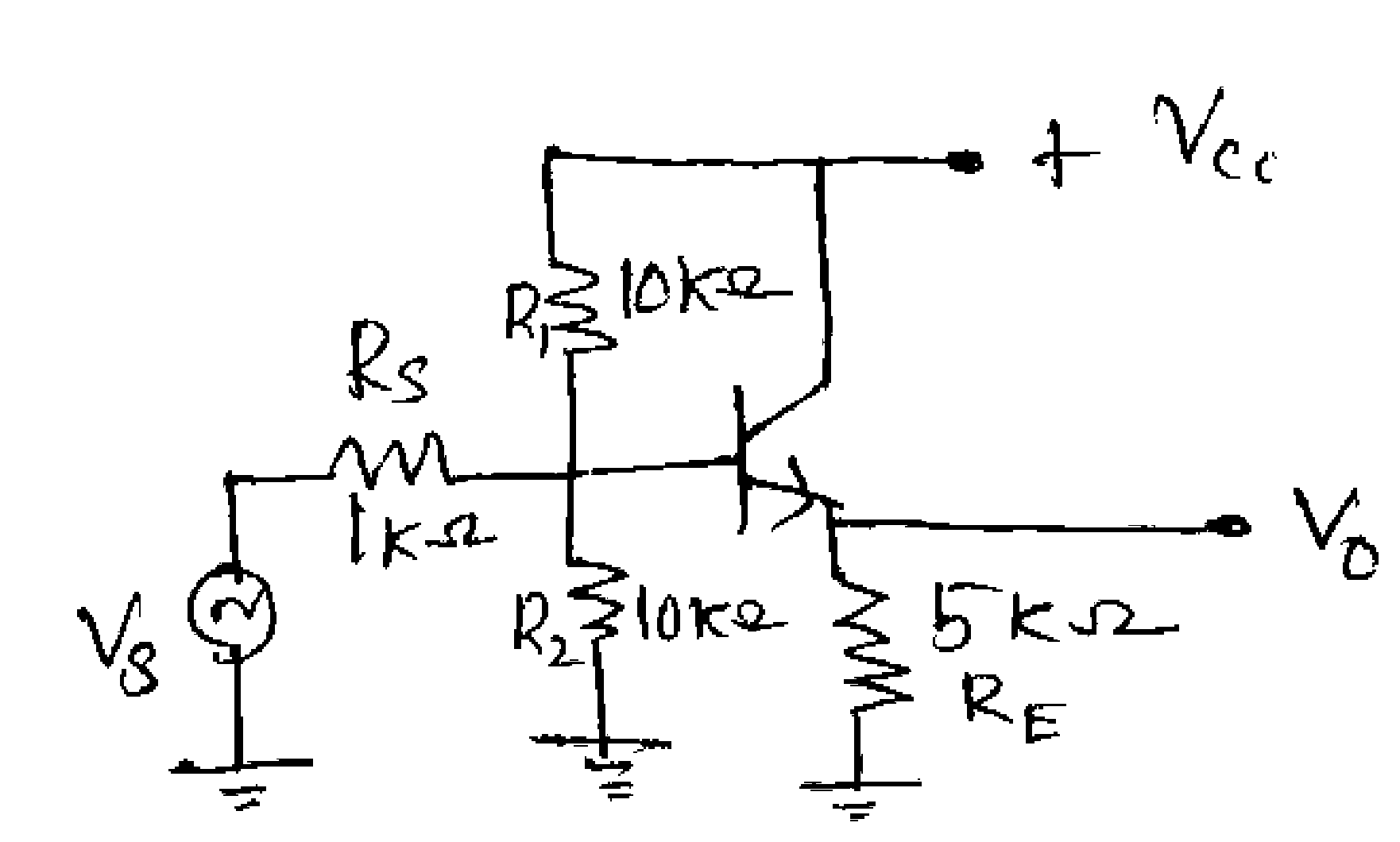
5. (a) What is the use of biasing?
(b) Draw the dc equivalent model.
(c) The circuit as shown in the figure 5c has fixed bias using NPN transistor. Determine the value of base current, collector current, and collector to emitter voltage. [4+4+8]
 |
|
Figure 5c |
6. A transistor used in a CB amplifier has the following values of h - parameters. hib= 28 Q, hfb = - 0.98, hrb = 510-4 and hob = 0.34x10⁻⁶S. Calculate the values of Ri, Ro, Ai and AV, if the load resistance is 1.2 KQ. Assume source resistance as zero.
[16]
7. Draw the practical circuit for voltage series feedback and find the voltage gain, input impedance & output impedance. [16]
8. (a) A colpitts oscillator is designed with C = 100 PF and C2 = 7500 PF. The
inductance is variable. Find the range of inductance value, if the frequency of oscillation is to vary between 950 KHz and 2050 KHz.
(b) A Hartely oscillator is designed with L2 = 20H and a variable capacitance. Find the range of capacitance values. If the frequency of oscillation is varied between 950 KHz to 2050 KHz. [10+6]
I B.Tech Supplimentary Examinations, Aug/Sep 2008 ELECTRONIC DEVICES AND CIRCUITS ( Common to Electronics & Communication Engineering, Computer Science & Engineering, Electronics & Instrumentation Engineering, Bio-Medical Engineering, Information Technology, Electronics & Control Engineering, Computer Science & Systems Engineering, Electronics & Telematics, Electronics & Computer Engineering and Instrumentation & Control
Engineering)
Time: 3 hours Max Marks: 80
Answer any FIVE Questions All Questions carry equal marks
1. Derive the expression for the deflection in an electrostatic deflection system. Hence obtain the expression for electro static deflection sensitivity. [16]
2. (a) Explain the volt ampere characteristics of PN diode.
(b) Explain the temperature dependence of VI characteristics. [8+8]
3. Derive the ripple factor of capacitor filter. [16]
4. (a) Define a Transistor.
(b) What are the differences between Bipolar Junction transistor & Field effect Transistor?
(c) Write any two applications of transistor. [5+7+4]
5. (a) What is the use of biasing?
(b) Draw the dc equivalent model.
(c) The circuit as shown in the figure 5c has fixed bias using NPN transistor. Determine the value of base current, collector current, and collector to emitter voltage. [4+4+8]
 |
|
Figure 5c |
6. Derive the expressions for voltage gain, current gain, I/P impedance, O/P impedance of CE amplifier, using exact & approximate model. [16]
[16]
[16]
7. With neat sketch explalin about all types of feedback systems.
8. Explain briefly about frequency and amplitude stability of oscillators.
2 of 2
|
Attachment: |
| Earning: Approval pending. |