Biju Patnaik University of Technology 2008-3rd Sem B.Tech Computer Science and Engineering of analog electronic circuit - Question Paper

i / number of printed pages -7 B. Tech
CPES 5202
hird Semester Examination - 2008 ANALOGUE ELECTRONICS CIRCUIT Full Marks-70
Time: 3 Hours
IWL
nswer Question No. 1 which is compulsory and any five from the rest.
The figures in the right-hand margin indicate marks.
Answer the following in brief. Provide suitable illustrations wherever necessary : 2x10
. (a) Draw the small signal hybrid model of a n-channel FET,
|
(b) |
Which h'parameters one can determine |
(h) Give the dc load tine for a fixed bias circuit . | |
|
from the input characteristics and the |
with V * 9 V, p =100 and R0 = 20 Kn cc D | ||
|
output characteristics of a BJT ? |
that uses a silicon transistor. | ||
|
(e) |
Write down two salient features of a |
(i) Which power amplifier has the maximum | |
|
voltage series feedback. |
efficiency for a given input power ? Why ? | ||
|
(d) |
What is the roll-off factor in a Bode plot? |
(j) What are the minimum values of gain in | |
|
Justify. |
IWL |
inverting and non inverting amplifiers ? | |
|
(e) |
Why is a fixed bias called so ? Justify, |
2. |
(a) Draw and analyze a circuit that can add |
|
four voltages of1 V, 1.5 V, 2 V and 2.5 V. | |||
|
(f) |
Prove that in a constant current source |
Find out the output voltage. State the | |
|
circuit current is indeed a constant. |
assumptions used. | ||
|
{g> |
Write down two advantages of a push-pull |
(b) Draw to scafe the output waveform of an | |
|
power amplifier. |
integrator when a square waveform of | ||
|
CPES 5202 2 Contd. |
CPES 5202 3 | ||
2V is applied to its input. Derive the formula used. 4
a (a)
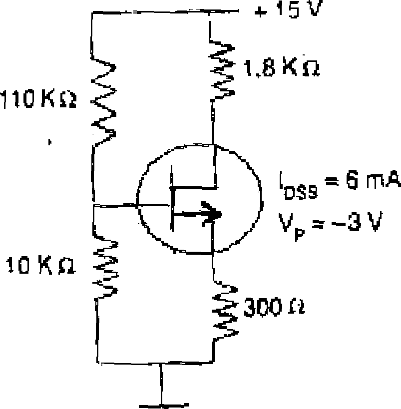
For the circuit shown above, draw the transfer characteristics. 6
|b) Fortfte circuit as shown in (a), find out VG,
Draw the d,c. load line. A
CPES 5202 A Cgntd.
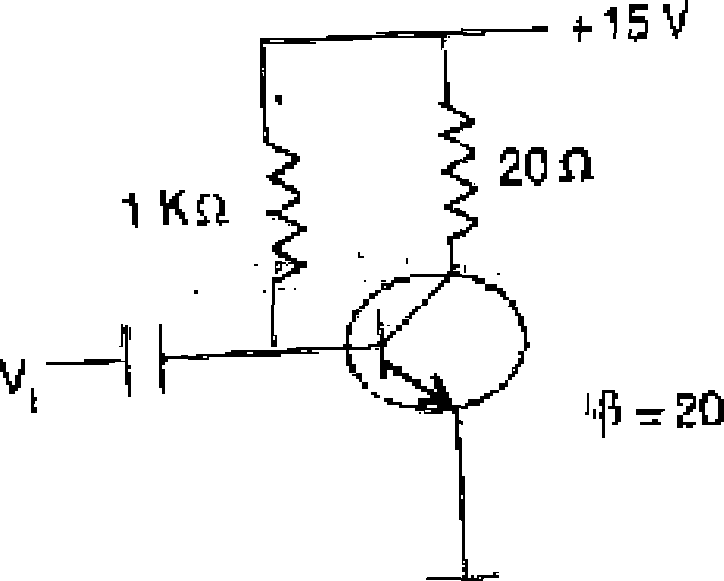
For the circuit shown above, determine Zlt Zo, A and A- using tine h-parameter model. Derive
V I
the formulae used.
IWL
5, (a) Derive the maximum efficiency of a series fed class A power amplifier. 5
[
l
, PJ.O.
CPES 5202
|
Fo' the arcuil shown in part (b), calculate |
0 |
(a) |
Explain frequency response of BJT |
|
me input power, thei output power and |
amplifiers 5 | ||
|
eJhcrency of The amplifier fOf an mpul |
(b) |
Draw and analyze a D-MOSFET | |
|
vottage resulting m a base current oft OmA |
configuration. Why is it called so? 5 | ||
|
peak 5 | |||
|
6, (a) Explain square wave testing of an | |||
|
amplifier. What information does it provide? I(VL | |||
|
(b) Explain a cascode configuration What is | |||
|
its utility ? 4 | |||
|
7. Derive the conditions for oscillation in a RC phase | |||
|
shift oscillator. What type of waveform does il |
* | ||
|
generate? 10 | |||
|
CPES 5202 6 Contd. |
CPES 5202 7 c | ||
|
Attachment: |
| Earning: Approval pending. |