Manipal University 2007 THIRD SEMESTER MAKE-UP (REVISED CREDIT SYSTEM) - Question Paper
ANALOG ELECTRONIC CIRCUITS (ELE 209)
Reg. No.:
MANIPAL INSTITUTE OF TECHNOLOGY, MANIPAL
(A Constituent Institute of MAHE, Deemed University)
THIRD SEMESTER B.E. DEGREE MAKE-UP EXAMINATION
(REVISED CREDIT SYSTEM)
16 January 2007
ANALOG ELECTRONIC CIRCUITS (ELE 209)
Time: 3 hours Max. Marks: 50
Note: Answer any FIVE full questions.
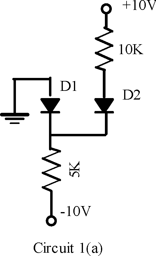
IA) Refer circuits 1(a), determine the current through D1 assuming ideal diodes. (02)
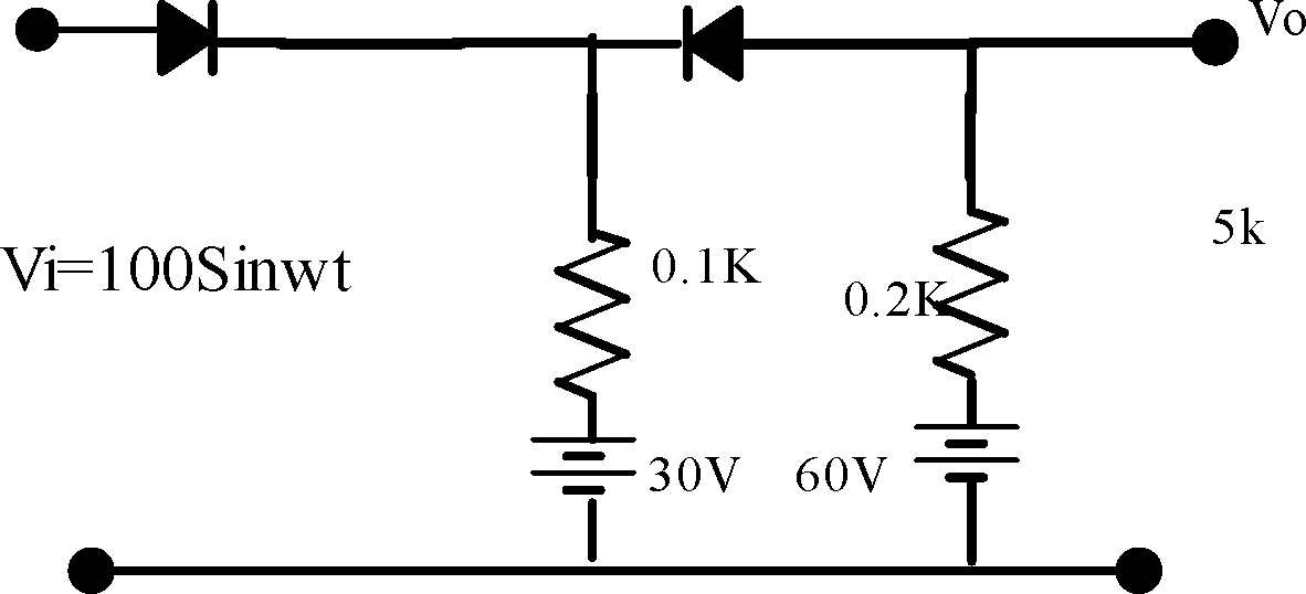
IB) For the circuit shown in fig (1b), plot the output waveform assuming Ge diode. (04)
IC) With suitable circuit diagrams and waveforms explain positive and negative clampers. (04)
2A) List two important features of i) Schottky diode ii) Photo diode (02)
2B) With neat diode switching characteristics, define the following terms.
Reg. No.:
i) reverse recovery time ii) transition time iii) storage time (03)
2C) Assume a silicon transistor with P=50, VBE=0.7V, Vcc=22.5V, Rc=5.6K is used. It is desired to establish a Q point at (12V, 1.5mA) and S=3.Dessign a self bias circuit. (05)
3A) State and prove Millers theorem. (02)
3B) Refer circuit (3b) Determine Ai, Av, Ri, Ro, Ristage, Rostage.Draw the h-parameter model. Given hie=1K,hre = 2.5*10-4, hoe= 24pA/V, hfe=50. (08)
4A) Derive an expression for overall current gain of a Darlington emitter follower Circuit (03)
4B In a current mirror circuit, if one transistor biases n transistors, what is the expression for the collector current? Derive the same. (03)
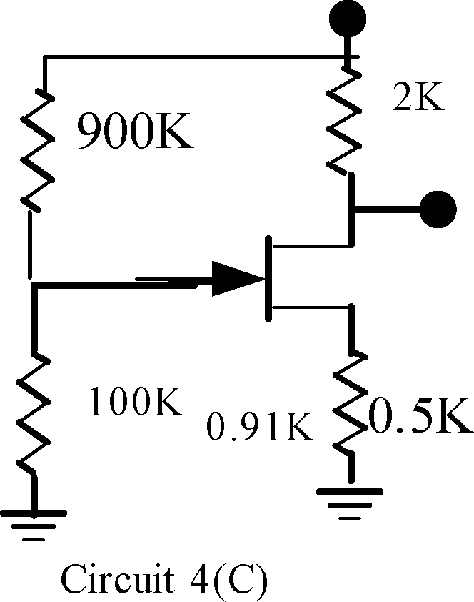
4C) Determine Vgsq,IDq,Vg,Vd,Vs,Vds for the circuit shown in fig (4C), IDSS=10mA,VP=-5V (04)
5A) Draw a circuit of a CMOS inverter and explain the working. (03)
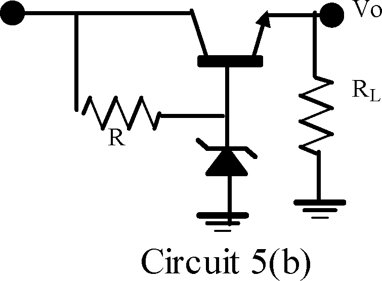
5B) Refer circuit(5B);VBE=0.7V,Vin can vary from 18V to 30V.If Vz=10V,R=500Q RL=1K, Determine i) the minimum collector to emitter voltage of the transistor. ii) the maximum power dissipated in the transistor. iii)The maximum current supplied by Vin. (03)
5C) A transformer coupled class A power amplifier having a collector supply voltage of 15V delivers an output of 3W to a load resistance of 1.5Q connected to a secondary of an ideal transformer. Determine the turns ratio and dc power input and efficiency of the transistor. (04)
6A) Classify the power amplifiers based on the operating point. (03)
6B) The voltage gain of an RC coupled amplifier decreases to 80%of its midband gain at 500 KHz .What is the upper 3 dB frequency of the amplifier? (03)
6C) An RC stage with R=33Q,C=120F is used to filter a signal of 24V dc with 2V rms operating from a full wave rectifier. Calculate the percentage ripple at the output of RC section for 100mA load,Asssume supply frequency is 50Hz. (04)
 |
|
Circuit(lb) |
+12V
9K-
-k:
 |
Vi |
5K
J1(-0 Vo
Circuit 3(b)
C
Vcc
Vin
|
Attachment: |
| Earning: Approval pending. |