Manipal University 2010 B.E Electronics & Communication Engineering University: ; : Computer Science and Engineering; Title of the : Basic Electronics (2011) - Question Paper
MANIPAL INSTITUTE OF TECHNOLOGY
Manipal University, Manipal – 576 104
SECOND SEMESTER B.E. DEGREE END SEMESTER exam
MAY-2010
SUBJECT: BASIC ELECTRONICS (ECE –101/102)
(REVISED CREDIT SYSTEM)
TIME: three HOURS MAX. MARKS: 50
Summary: This is a make up ques. paper of 2010 of the subject "Basic Electronics" which will help the students to expertise their knowledge and skills on this subject.
|
Reg. No. |
MANIPAL INSTITUTE OF TECHNOLOGY


Manipal University, Manipal - 576 104 SECOND SEMESTER B.E. DEGREE END SEMESTER EXAMINATION
MAY-2010
SUBJECT: BASIC ELECTRONICS (ECE -101/102)
(REVISED CREDIT SYSTEM)
MAX. MARKS: 50
TIME: 3 HOURS
Instructions to candidates
Answer ANY FIVE full questions.
Missing data may be suitably assumed._
IA. Explain why cut-in voltage of silicon diode is higher than the cut-in voltage of Germanium diode.
IB. Simplify the following Boolean expression and realize the function using minimum number of NAND_gates_ _ _ _ _ _ __
A B C D + A B C D + A B C D + A B C D + A B C D + A B C D + A B C D + A B C D
IC. For a Zener network Rs = 520Q, V Z = 15V, Vi = 25 5V. Find the minimum and maximum value of RL so that the Zener diode remains in the ON state. IZmin = 1mA, PzMax = 8W. (2+4+4)
2A. Draw the load line of a self bias circuit. Also write the equation of the load line.
2B. Starting from fundamentals derive the expression for ripple factor and rectification efficiency of a full wave bridge rectifier. Also draw the circuit of the full wave bridge rectifier.
2C. Starting from fundamentals derive voltage expression for FM signal. (2+5+3)
3A. Draw the equivalent circuits of Ideal and Non ideal OPAMP.
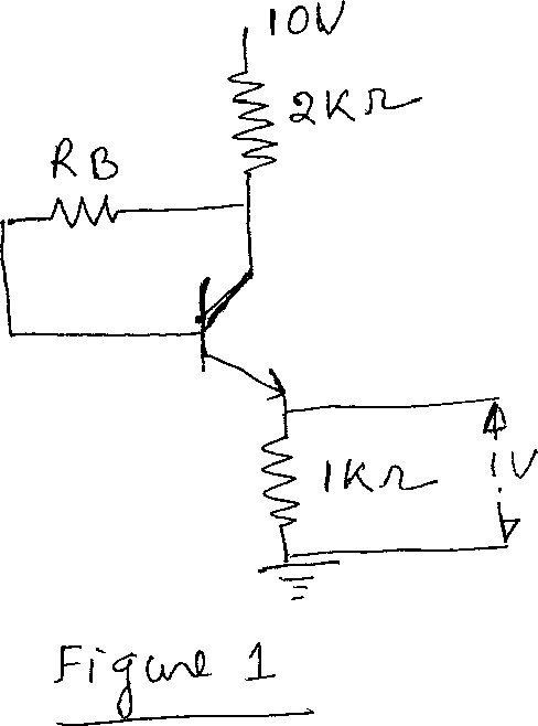
3B. For the circuit shown in figure 1 determine the DC operating point. Transistor used is a silicon transistor with VBE = 0.7V and P = 50.
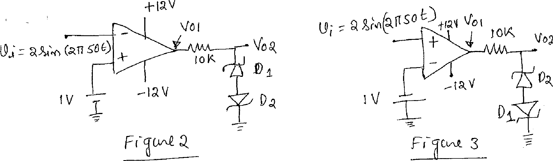
3C. For the circuits shown in figures 2 & 3 Sketch the voltages Vo1 & Vo2 with reference to Vi. The Diodes used in the circuits are ideal Zener diodes with break down voltages of 2 V and 3 V for D1 and D2 respectively. (2+4+4)
4A. Explain the need for modulation in communication systems.
4B. Realize each of the following equations using single OPAMP. Draw the circuit diagram, derive the input output relationship and determine the component values.
(i) Vo = -2V1+2V2 + V3
(ii) Vo = -2V1 - 4V2 + 7V3.
4C. With equations explain a dc, aac, P dc , Pac, Icbo & Iceo. (2+5+3)
5A. For the Zener Regulator Vi = 16 V, RS = RL = 1KD, VZ = 12 V. Determine V0, IZ, PZ. Also draw the circuit of the Zener Regulator.
5B. Indicating the direction of currents and polarity of voltages draw the input and output V-I characteristics of a PNP transistor in CE mode and explain.
5C. With equations explain drift and diffusion currents in semiconductors. (2+5+3)
6A. Compare Zener and Avalanche breakdown.
6B. Perform the following:
i) (F69.D3)16 + (325.67)8 = (?)i6
ii) (13.25)10 - (26.75)10 = (?)1ousing Binary 2s complement arithmetic.
6C. i) For what voltage will the reverse saturation current in a p-n junction germanium diode reaches 70% of its saturation value at room temperature? Assume room temperature of 27C
ii) What is the ratio of current for a forward bias of 0.05 V to the current for the same magnitude of reverse bias? (2+4+4)
ECE -101/102 Page 2 of 2
|
Attachment: |
| Earning: Approval pending. |