Manipal University 2009-3rd Sem B.E Electrical and Electronics Engineering Analog Electronic circuits for EEE - Question Paper
The papers are attached.
Department of Electrical and Electronics Engineering
Reg. No. :
MANIPAL INSTITUTE OF TECHNOLOGY, MANIPAL
(A Constituent Institute of Manipal University, Manipal)
THIRD SEMESTER B.E. DEGREE MAKEUP EXAMINATION
(REVISED CREDIT SYSTEM)
22 July 2009
ANALOG ELECTRONIC CIRCUITS (ELE 209)
Time: 3 hours Max. Marks: 50
Note : Answer any FIVE full questions.
Missing data, if any, may be suitably assumed.
IA. Determine Id, Vo for the circuit shown in Figure Q1A, given Vd=0.7V. (02]
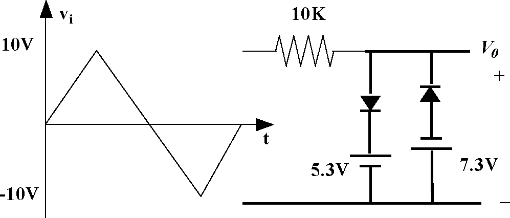
IB. D raw the output voltage for the circuit shown in Figure Q1B. (06]
IC. Write a technical note on construction and applications of photo diode. (02]
2A. Plot the waveform of Vo, for the circuit shown in Figure Q2A. (02]
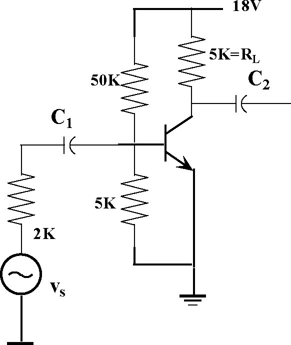
2B. Design a voltage divider bias circuit to meet the following specifications. Vcc=24V, Vce=4.5V, Ic=10mA, pdc=100, S(Ico]<5, Re=280H. (04)
2C. Derive the expression of stability factor S(Ico) and S(Vbe) for collector-base feedback bias circuit. (04)
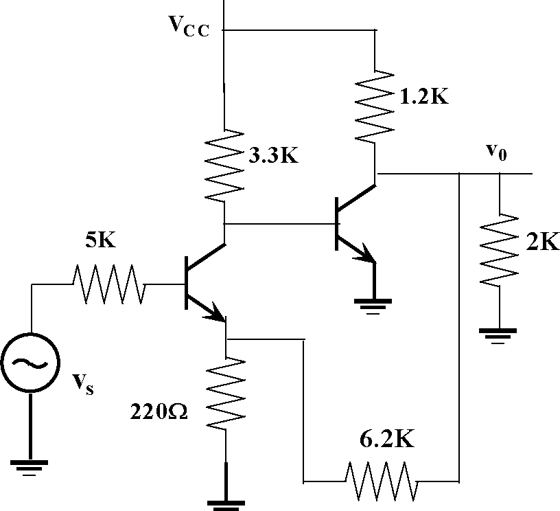
3A. Draw the low frequency small signal h-parameter model for the circuit shown in figure Q3A. Also identify the configuration employed in the circuits for both transistors. (02) 3B. For the circuit shown determine Av, Avs, Ro and R;. Given hie=1.1K, hre=2.5x10⁻⁴, hf=50, ho=24A/V. (04)
3C. Derive expression for calculating the voltage gain Av, current gain Ai, input impedance Zi and output admittance Yo of an amplifier using hybrid parameters. (04)
4A. Discuss the effect of cascading of amplifiers on bandwidth and gain. (02)
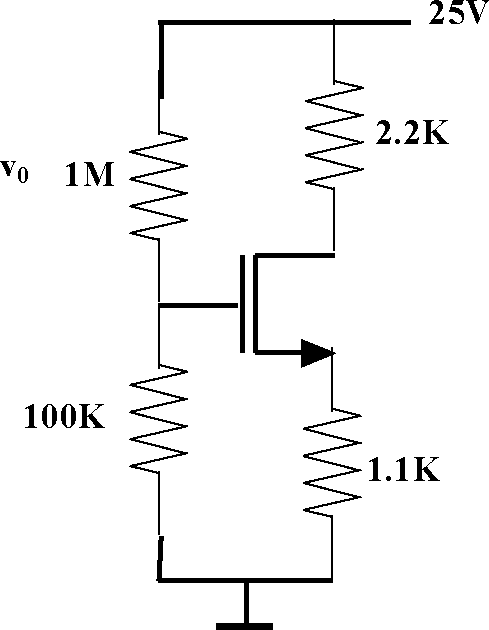
4B. For the network shown in Figure Q4B, find Vg, Idq, Vgsq, Vd, Vs and Vdsq. Given lDss=10mA, Vp=-4V. (04)
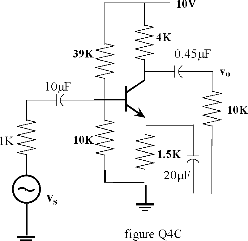
4C. For the CE amplifier shown in Figure Q4C, determine the bandwidth if hie=1.2K, hfe=100, ro=OT. (04)
5A. Write a brief note on distortion in power amplifiers (02)
5B. For a transformer coupled class-A power amplifier, derive an expression for efficiency and hence obtain maximum efficiency. Also list advantages and disadvantages of the same. (04)
5C. A series fed class A amplifier has Rb=2K, Rc=20H, |3=25 and Vcc=25V. Draw the circuit and determine DC input power, efficiency, and power dissipated. Assume the peak value of base current due to AC input voltage is 10Ma. (04)
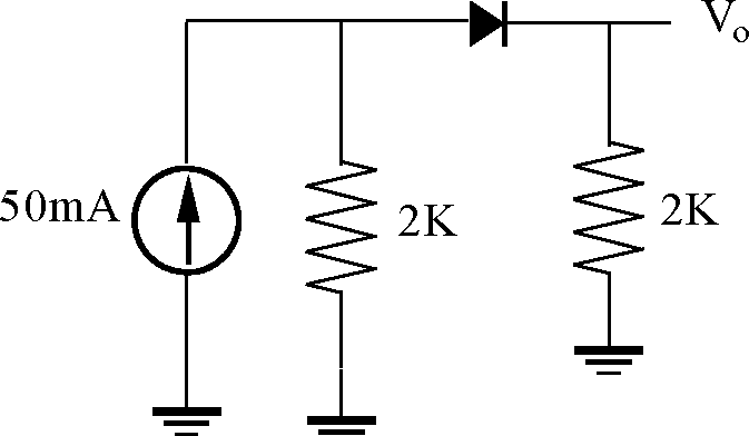
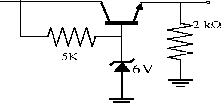
6A. Determine the output power and Zener diode current for the circuit shown in Figure Q6A. Given p=75. (02)
6B. Explain the working of a transformer based series voltage regulator. (04)
6C. Design a LM317 based variable voltage regulator for 5 to 15V range supplying not more than 100mA load current. (04)
 |
|
Figure Q1B |
 |
|
figure Q3A |
|
Id- |
 |
|
figure Q1A |
 |
|
figure Q2A |
 |
|
Figure Q3B |
 |
|
figure Q4B |
Vi = 20 V
|
Vn |
 |
|
figure Q6A |
Department of Electrical and Electronics Engineering
MANIPAL INSTITUTE OF TECHNOLOGY, MANIPAL
(A Constituent Institute of Manipal University, Manipal)
THIRD SEMESTER B.E. DEGREE END SEMESTER EXAMINATION
(REVISED CREDIT SYSTEM)
11 December 2010 ANALOG ELECTRONIC CIRCUITS (ELE 209)
Time: 3 hours_Max. Marks: 50
Note : Answer any FIVE full questions. Refer Table-1 for h-parameters.
IA. Determine Vo for the circuit shown in Fig 1(A).
(02)
(03)
(05)
(03)
(04) (03)
(05) (05)
IB. Define Transition time, storage time and reverse recovery time with respect to a PN junction diode
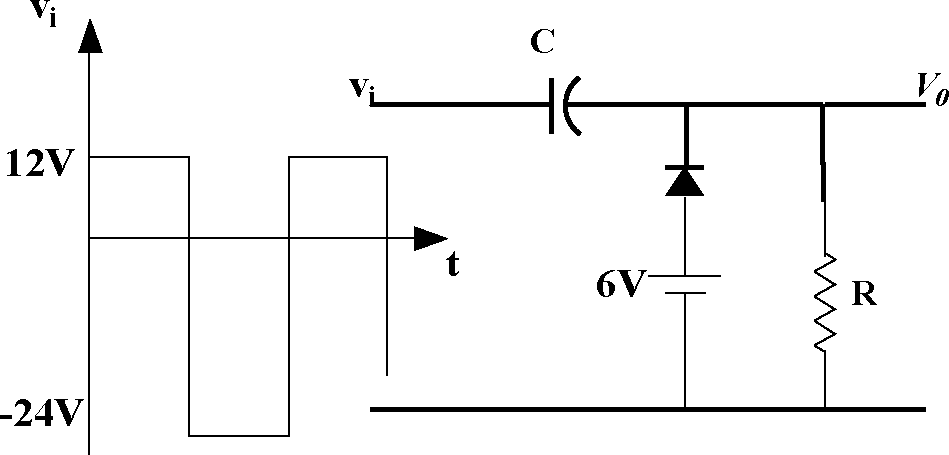
IC. Plot the waveform by determining V0 for the circuit shown in Fig 1(C).
2A. Determine the transistor quiescent voltages and currents of the amplifier shown in Fig 2 (A). Assume Vbe=0.7V.
2B. From the fundamental derive an expression for S(Icbo), for voltage divider biasing circuit with emitter resistance RE.
2C. Draw the small signal h- parameter model of a Darlington pair transistor connection. Hence list out its merits and demerits.
3A. Design a voltage divider biasing circuit to meet the following specifications, VCC=25V, Vce=4V, Ic=10mA, P = 100 , S - 5 and RE=100n. Hence draw the circuit.
3B. For the cascaded amplifier shown in Fig 3(B) determine Av, Avs = v0/vs, and Ri using approximate h-parameter transistor model.
10, C 200 fA I v .Determine
W
L
4A. An NMOS has V ~ 0.5V and
i. The value of the Vgs to operate in saturation region with a dc current Idc=100itiA.
ii. Value of the Vgs required to cause the device to operate 1000Q resistor for very small ac, vds signal.
w , j
The MOSFET shown in Fig. 4(B) has }inCDX = (SAmA/V , Vt=lV, ro=40K. Determine all the quiescent
current and voltages and hence determine the output voltage when sinusoidal vi=0.8mv is applied at the input of the amplifier.
Derive an expression for current gain, the input resistance and output resistance of a single common gate MOSFET amplifier
(02)
(04)
(04)
4B.
4C.
5A.
5 (A), both
Uf
100 and the drain current of
L:_
MOSFET M2 =lD2=2mA. Determine
i. The quiescent Vgs and Vds of both the MOSFETs and aspect ratio ()ofM2
ii. Draw the small signal equivalent circuit and hence find small signal voltage gain from vs to vo.
iii. Maximum sinusoidal input that can be applied before the output begin to clip.
For a transformer coupled class A power amplifier, derive an expression for efficiency and hence obtain maximum efficiency. Also list any two disadvantages of the same.
Determine the lower and upper cut off frequency of the CE amplifier shown in Fig 6(A). Hence find the band width. Assume the R0=50K, Cx=1F, C2=4F, C0=1nf and Ce=10F.
Determine the output voltage V0, Vce and currents through all the resistance in the circuit shown in Fig. 6(B), where Vbe = 0.7 V
Design a 7805 variable voltage regulator to get an Output voltage range 6V to 16V. Take R1 = 1K, Iadj=4.3mA. Draw the circuit.
In the amplifier shown in the circuit Fig
the MOSFETs are having Vt=0.7V, w.
~ 20x2 ~ 500i*A/V2, aspect ratio of MOSFET Ml=y=
(06)
(04)
(04)
(04)
(02)
5B.
6A.
6B.
2K Dl
2K
|
C =100J.LS | |
 |
V |
|
Fig 1(A) | |
HAM
-VVWHVWV-
 |
t V |
D 3
6V
4K
Vo
D
4K
4 V
Fig 1(C)
 |
|
Fig 3(B) |

 |
V 0 |
|
Fig 2(A) | |
 |
|
Fig 4(B) |
 |
|
Fig 6(A) |
|
h-parameters |
CE |
CB |
CC |
|
hi |
1.1K |
1.1K |
21.6 ohms |
|
hr |
2.5x10⁻⁴ |
1 |
2.9x10⁻⁴ |
|
hf |
50 |
-51 |
-0.98 |
|
ho |
24|jmho |
25jmho |
0.49jmho |
 |
|
Fig. 6(B) |
Page 2 of 2
|
Attachment: |
| Earning: Approval pending. |