Maharashtra State Board of Technical Education 2008 Diploma Electronics & Video Engineering Principles of Digital Techniques - Question Paper
Sample Question Paper - I
:- Electronics Engineering group :- EJ/EN/EX/IS/MU/IE/IC/DE/ EV/ED/EI :- Third
Course Name Course code Semester Subject Duration
:- Principles of Digital Techniques :- 3 hours
Marks: 80
Instructions :
1] All questions are compulsory.
2] Figures to the right indicates full marks.
3] Use of non-programmable calculator is permissible.
Q 1: Attempt any Eight of the following :
1. Define universal gate. Give example of each.
2. Mention any four Boolean laws.
3. Specify the function of following ICs
IC 74150, IC 74151, IC 74153, IC 74157.
4. What is the necessity of demultiplexer?
5. Write the truth table of D & T flip flop.
6. Draw the one bit memory cell using NOR gate.
7. Define the following terms
i) Propagation delay.
ii) Fan - out.
8. What is the purpose of pull - up resistor in TTL logic family?
9. Draw the circuit diagram of 2:1 multiplexer.
10. If F = X + XY find the complement of F.
Q.2 : Attempt any three of the following; Marks: 12
1. Convert the following decimal no into Binary octal. Hexadecimal and BCD equivalent. (120.65).
2. Simplify the following expression with Boolean laws,
i) Y = (B + BC) (B + C) (B + D).
ii) Y = ABC (ABC + ABC + ABC)
3. Minimize the following expression using K-map.
F (A, B, C, D) = Xm (0,1,2,3,4,5,7,8,9,11,14).
4. Describe the drawback of JK FF. Also state how to eliminate the same.
Marks: 16
Q.3: Attempt any three of the following. Marks: 12
1. Compare the Combinational and sequential circuit based on its characteristics.
2. Design 3 bit synchronous up counter using T FF with the help of timing diagram.
3. Compare characteristics of TTL & COMS logic family. (Min. 4 points).
4. Draw 1:64 demultiplexer tree using only 1:16 demux.
Q.4: attempt any two of the following. Marks: 16
1) A i) Draw the output wave forms for following condition,
a) Positive edge triggered D FF.
b) Negative edge triggered JK FF.
CLOCK
INPUT
ii) Design MOD - 20 counter using IC 7490 and describe the working of same.
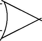
B) i) Write the sop expression for the below circuit diagram.
ii) Which is the fastest logic family out of all logic families and why?
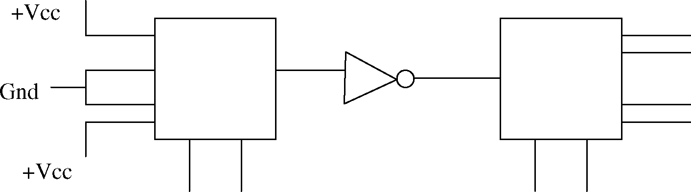
iii) Draw the pin out diagram of IC7408.
iv) Subtract the following number using 2s complement.
(12)10 - (15)10
C) i) Give the excitation table of SR flip- flop.
ii) Give any two differences between multiplexer & demultiplexer.
iii) Give the value of any two characteristics of TTL.
iv) Draw CMOS inverter.
Q.5: Attempt any three of the following. Marks: 12
A) i) Add the following BCD no.
(9)10+ (4)10
ii) Subtract the following no using 10s complement.
(16) 10 - (8)10
B) Design the 3 bits a synchronous down counter using T FF with the help
of Timing diagram.
C) In the given diagram the control signal A, B changes from 00 through 11. Write the truth table.
A B A B
D) Realize the full adder using K-map technique.
Q.6: Attempt any three of the following. Marks: 12
a. Realize EX-OR gate using NAND gate only & derive the expression for
same..
b. Draw the circuit diagram of 4-bits (SIPO) shift resistor with the timing diagram.
c. Give the function of following ICs & draw the pin diagram IC 7474.
d. Write the truth table of IC 74138 & Describe the same.
|
Attachment: |
| Earning: Approval pending. |