Deemed University 2011 B.Tech Electronics and Communications Engineering University: Lingayas University Term: V Title of the : Electrical Engineering Materials and Semi-Conductor Devices - Question P
Roll No. ..
Lingayas University
B.Tech. 2nd Year (Term V)
Examination Feb 2011
Electrical Engineering Materials and Semi-Conductor Devices (EC - 202)
[Time: 3 Hours] [Max. Marks: 100]
![]()
Before answering the question, candidate should ensure that they have been supplied the correct and complete question paper. No complaint in this regard, will be entertained after examination.
![]()
Note: All questions carry equal marks. Attempt five questions in all. Question no. 1 is compulsory. Select two questions from Section B and two questions from Section C.
Section A
Q-1. Part - A
Select the correct answer of the following multiple choice questions. (10x1=10)
(i) What kind of device is a resistor?
(a) Unilateral (b) Nonlinear
(c) Linear (d) Bipolar
(ii) An electron in the conduction band
(a) Is bound to its parent atom
(b) Has no charge
(c) Is located near the top of the crystal
(d) Has higher energy than an electron in the valence band
(iii) Forbidden energy gap at 300K for Si and Ge respectively are
(a) 1.21 eV and 0.785 eV
(b) 1.1 eV and 0.72 eV
(c) 0.785 eV and 1.21 eV
(d) 0.72 eV and 1.1 eV
(iv) The width of depletion layer of PN junction
(a) Increases when forward biased
(b) Reduces with forward biased
(c) Increases with heavy doping
(d) Is independent of applied voltage
(v) The relationship between electric flux density D and electric field E in a dielectric is
(a) D = ![]() (b)
D = -
(b)
D = - ![]()
(c) E = ![]() (d)
E = -
(d)
E = - ![]()
(vi) The surface over which Gausss law is applied must be
(a) Closed (b) Open
(c) Closed and open (d) None
(vii) The relationship between magnetic flux density B and magnetic field H
(a) B = ![]() (b)
B = -
(b)
B = -![]()
(c) B = ![]()
![]() (d)
B = -
(d)
B = - ![]()
(viii) In an intrinsic semiconductor
(a) There are no holes in the material (b) The number of holes is too small
(c) Electrons in the material are neutralized by holes (d) there are no electrons in the material
(ix) The components of current across a forward biased PN junction are
(a) Drift current (b) Diffusion current
(c) Drift and diffusion current (d) None
(x) The creation of a very large magnetization in a material when magnetic field is applied is called
(a) Para-magnetic (b) Diamagnetic
(c) Ferro-magnetic (d) Anti ferromagnetic
Part B
(i) Explain Gausss theorem for electric field.
(ii) Explain magnetic susceptibility.
(iii) Why BJT is called current controlled device?
(iv) What is pinch-off voltage in a JFET?
(v) Why FET is called a voltage controlled device. (5x2=10)
Section B
Q-2. (a) Explain electronic polarization, ionic polarization and orientational polarization of dielectrics clearly.
(b) Explain the term electrostriction and magnetostriction with its application. (2x10=20)
Q-3. (a) What is LED? Give its principle of working, construction, symbol, merit, demerits and applications.
(b) What is photodiode? Give its biasing arrangement and construction. How does it operate? Explain it with its applications. (2x10=20)
Q-4. (a) Draw the structure of a JFET and explain its principle of operation with neat diagram along with its V-I characteristics. Define pinch-off voltage and symbol clearly.
(b) Describe clearly the construction, operation and V-I characteristics of a Depletion type MOSFET. (2x10=20)
Section C
Q-5. (a) Explain Drift velocity and mobility of a free electron. A conduction wire has a resistivity of 1.54* 10-8 W-m at room temperature. There are 5.8 * 1028 conduction electrons per m3. Calculate the mobility and relaxation time of electrons.
(b) Explain superconductivity. The material lead (Pb) behaves as a superconductor at a temperature of Tc = 7.26 K. If the value of critical magnetic field of lead at T = 0 K is Hc = 8 * 105 A/m, find the critical magnetic field of lead at 4 K. (2x10=20)
Q-6. (a) Find the magnitude of flux density in a material for which
(i) The magnetization is 2.8 A/m and the magnetic susceptibility is 0.0025.
(ii) The magnetic field intensity is 1,300 A/m and the relative permeability is 1.006.
(iii) There are 8.2 * 1028 atoms/m3, each having a dipole moment of 3 * 10-30 A-m2 in the same direction and the magnetic susceptibility is 2 * 10-4.
(b) Explain Hysteresis loss. Calculate the loss of energy caused by hysteresis in one hour in 50 kg of iron if the peak flux density reached is 1.3 T (Wb/m3) and the frequency is 25 Hz. Assume Steinmetz coefficient as 628 J/m3 and density of iron as 7.8 * 103 kg/m3. (2x10=20)
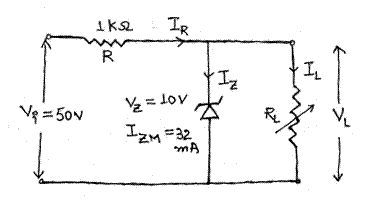
Q-7. (a) What is Zener effect? Determine the range of RL and IL that will result in VL being maintained at 10 v.
(b) Define drift and diffusion current in a
semiconductor. Find the conductivity and resistivity of an
intrinsic semiconductor at temperature
of 300 K. Given ni=2.5 * 1013/cm3,
![]() =
3800 cm2 / V-s,
=
3800 cm2 / V-s, ![]() =
1800 cm2 / V-s, e = 1.6 * 10-19
C. (2x10=20)
=
1800 cm2 / V-s, e = 1.6 * 10-19
C. (2x10=20)
Q-8. (a) Explain the basic construction of a silicon controlled rectifier (SCR). The gate current in a Thyristorized half wave rectifier is adjusted to 1.25 mA and the forward breakdown voltage of SCR corresponding to this gate current is 110 V. The applied voltage is 220V, the load resistance is 150W and the holding current is zero. Determine (i) firing angle (ii) conduction angle (iii) average output voltage (iv) average current and (v) power output.
(b) Explain the basic construction of UJT. Sketch its V-I characteristics and explain its operation. (2x10=20)
| Earning: Approval pending. |