Deemed University 2011 B.Tech Electronics and Communications Engineering University: Lingayas University Term: V Title of the : Analog Electronics - Question Paper
Roll No. ..
Lingayas University
B.Tech. 2nd Year (Term V)
Examination Feb 2011
Analog Electronics (EC - 205)
[Time: 3 Hours] [Max. Marks: 100]
![]()
Before answering the question, candidate should ensure that they have been supplied the correct and complete question paper. No complaint in this regard, will be entertained after examination.
![]()
Note: Attempt five questions in all. All questions carry equal marks. Question no. 1 is compulsory. Select two questions from Section B and two questions from Section C.
Section A
Q-1. Part A
Select the correct answer of the following multiple choice questions. [10x1=10]
(i) The input impedance of a JFET is of the order of
(a) 100 MW (b) 1 MW (c) 100W (d) 10W
(ii) The early effect in Bi-polar Junction Transistor is caused by
(a) Fast Turn-on (b) Fast Turn-off
(c) Large collector base reverse bias
(d) Large emitter base forward bias
(iii) The pinch-off voltage of a JFET is 5 V. Its cut-off voltage is
(a) (5.0)1/2 (b) 2.5 v (c) 5.0 v (d) 0 v
(iv) The primary reason for the wide-spread use of Silicon in semiconductor device technology is
(a) Abundance of silicon on the surface of the Earth.
(b) Largei band-gap of silicon in comparison to Germanium.
(c) Favorable properties of Silicon Di-Oxide (SiO2).
(d) Lower Melting point.
(v) If bdc is increased by 10%, the collector to emitter voltage drop
(a) Increases by less than or equal to 10%
(b) Decrease by less than or equal to l0%
(c) Increases by more thanl0%
(d) Decrease by more than l0o/o
(vi) When an n-channel depletion type MOSFET are used in enhancement mode
(a) The gate will be positive
(b) The gate will be negative
(c) The gate will be at ground level
(d) None of these
(vii) For good stabilized biasing of the transistor of the voltage divider CE amplifier, which condition should be satisfied:
(a) RE/ RB << 1 (b) RE/ RB >>1
(c) RB/ RE << hi (d) RB/ RE >> hi
(viii) The main component responsible for the fall of an RC-coupled amplifier in the low frequency range is
(a) The active device itself (b) stray shunt capacitor, Cs
(c) coupling capacitor cc (d) the collector grid-leak resistor, Rc
(ix) NPN Transistors are preferred over PNP counterparts due to their better
(a) High frequency response (b) Low frequency response
(c) Mid range frequency response (d) None
(x) The emitter resistor Re bypassed by a capacitor CE
(a) reduces the voltage gain (b) causes the thermal runaway
(c) increases the voltage gain (d) stabilizes the Q-point'
Q-1. Part B
(i) The stability of a system is a measure of the sensitivity of a network to variations in its parameters. Define those parameters change with respect to Ic sensitivity. (5)
(ii) In what ways the re model or hybrid model helps the designer to make a good design? Justify with three points. (5)
Section - B
Q-2. (a) Explain the switching characteristics of the PN junction with Diagram. Also comment upon heavily doped PN Junction switching behavior in comparison w.r.t. PN Junction Diode. (10)
(b) Draw the schematic circuit diagram of a six-fold voltage multiplier. Assuming ideal diodes and identical capacitors of 10mF each, calculate the equivalent capacitance across the output terminals of the multiplier. (10)
Q-3. (a) For a Full wave Bridge Rectifier circuit, derive Irms and instantaneous value of r.m.s, I'rms for one cycle. Also derive for Ripple factor (r) and rectification efficiency (h) for full wave bridge rectifier. (10)
(b) Explain why the gain of a CE Amplifier falls at low frequencies and also at high frequencies. Give point with reasons. (10)
Q-4. (a) Explain with block diagram working principle and features of SMPS. (10)
b) Explain the features and advantages of VMOSFET over planar MOSFET. (10)
Section - C
Q-5. (a) Analyze the common-emitter amplifier circuit with self biasing using h-parameters also drive the expression for input impedance, output impedance, current gain and voltage gain. (10)
(b) Explain Hybrid -fI model and what is the utility of this model at high frequencies? (10)
Q-6. (a) Draw the hybrid or fe model for the emitter follower circuit and find its voltage gain. Also write the application for which it is popularly used. (10)
(b) Draw the circuit of Common Source amplifier and draw it characteristics and its FET model. Also show the overall gain if RL is present. (10)
Q-7. (a) Explain Ebers -Moll Model and prove (10)
a1 . ICO = aN . IEO
(b) Explain working principle and operation of MOSFET with neat diagram. Explain with the concept of Accumulation, Depletion and
inversion in MOS Capacitor. (10)
Q-8. (a) Draw the circuit of Source Follower and its FET model. Also show the overall gain if output is taken across RL. Also explain whether the gain is more than CS amplifier or not. (10)
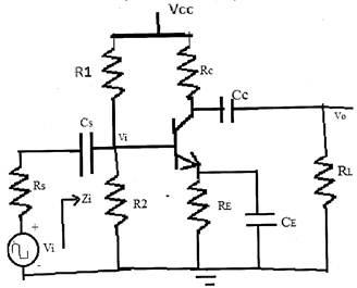
(b) Determine the lower cut-off frequency, gain at cut-off frequency, (Avf1), Zi, Avs, fLCs for the below network (fig. 8b) using following parameters: (10)
Cs=10 mF, CE=20 mF, Cc=1 mF, Rs= 1kW, R1=40 kW, R2=10 kW, RE = 2kW, Rc=4 kW, RL=2.2 kW, b= 100, ro = , Vcc=20V
| Earning: Approval pending. |