Deemed University 2011 B.Tech Electrical and Electronics Engineering University: Lingayas University Term: V Title of the : Semiconductor Materials
Roll No. ..
Lingayas University
B.Tech. 2nd Year (Term V)
Examination Feb 2011
Semiconductor Materials & Devices (EE - 203)
[Time: 3 Hours] [Max. Marks: 100]
![]() Before
answering the question, candidate should ensure that they have been supplied
the correct and complete question paper. No complaint in this regard, will be
entertained after examination.
Before
answering the question, candidate should ensure that they have been supplied
the correct and complete question paper. No complaint in this regard, will be
entertained after examination.
![]()
Note: Attempt five questions in all. All questions carry equal marks. Question no. 1 is compulsory. Select two questions from Section B and two questions from Section C.
Section A
Q-1. Part A
Select the correct answer of the following multiple choice questions. [10x1=10]
(i) As per Hall effect, if any specimen carrying a current-I is placed in a transverse magnetic field B, then an electric field E is induced in the specimen in the direction
(a) Parallel to I (b) Parallel to I and B
(c) Perpendicular to both I and B
(d) Perpendicular to B and parallel to I
(ii) A function FET can be used as a voltage variable resistor
(a) For any value of VDS
(b) Well below pinch-off condition
(c) Beyond pinch-off voltage
(d) At pinch-off condition
(iii) In a material, the Fermi level is located between the centre of the forbidden band and the conduction band. Then what is that material?
(a) An insulator
(b) An intrinsic semiconductor
(c) A p-type semiconductor
(d) An n-type semiconductor
(iv) Why npn transistors are preferred over pnp transistors?
(a) Bias voltage required in npn is greater than in pnp transistors.
(b) Bias voltage required in npn is less than m pnp transistors.
(c) Mobility of majority carries in npn transistors is greater than the mobility of majority carries in pnp transistors.
(d) Leakage current in npn transistors is less than pnp transistors.
(v) For a npn transistor, what is the main stream of current in the base region?
(a) Drift of holes (b) Diffusion of holes
(c) Drift of electrons (d) Diffusion of electrons
(vi) Consider the following statements:
FETs when compared to BJTs have
1) High input impedance
2) Current flow due to majority carriers
3) Low input impedance
4) Current flow due to minority carriers.
Which of the statements given above are correct?
(a) 1 and 4 (b) 2 and 3
(c) 3 and 4 (d) 1 and 2
(vii) The maximum peak-to-peak output voltage swing is obtained when the Q-point of a circuit is located
(a) Near cut off point (b) Near saturation point
(c) At the centre of the load line (d) Atleast on the load line
(viii) The main use of an emitter follower is
(a) Impedance matching (b) Power amplifier
(c) Low input impedance circuit (d) Follower of base signal
(ix) CE amplifier is characterized by
(a) Very high output impedance
(b) Signal phase reversal
(c) Low voltage gain
(d) Very high input impedance
(x) LED emits light of a particular colour because
(a) It is fabricated from a fluorescent material
(b) Transition between energy levels of the carriers takes place while crossing the p-n function.
(c) Heat generated in the diode is converted into light.
(d) The band gap of the semiconductor material used in the fabrication of the diode is equal to the energy hv of the light photon.
Part B
(a) State Millers Theorem and give its applications. [5]
(b) Explain how a zener diode can be used as a voltage regulator. [5]
Section B
Q-2. (a) Explain the difference between
(i) Drift and diffusion
(ii) Intrinsic and extrinsic semiconductors
(iii) Mobility and conductivity
(b) Mobilities of electrons and holes in a sample of intrinsic germanium at room temperature are 0.36 m2/v-s and 0.17 m2/v-s respectively. If the electron and hole densities are each equal to 2.5x10⁻¹⁹m3, calculate germanium conductivity. [2x10=20]
Q-3. (a) Draw the energy band diagram of an intrinsic, p-type and n-type semiconductors. Also draw it for p-n diode and indicate the barrier potential, depletion region, fermi level etc.
(b) Discuss Hall effect and its applications. [2x10=20]
Q-4. (a) Draw the V-I characteristic of a p-n diode and explain why the current in the forward bias does not start from can we measure the barrier potential of a p-n diode with the help of a multimeter? Justify your answer. [8]
(b) Explain the principle of operation of LED. [6]
(c) Explain the mechanisms of breakdown in p-n diodes. [6]
Section C
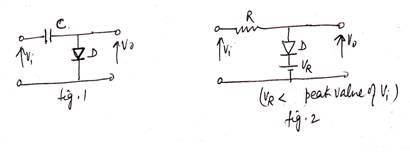
Q-5. (a) Draw the circuit of a bridge rectifier. Explain the role of capacitor as a filter element.
(b) Draw the output to the scale of the input for the two circuits given below (fig. 1 & 2) when the input is a sinusoidal signal. Assume ideal diode. [2x10=20]
Q-6. (a) Explain the n-p-n BJT action. Can a BJT be made by connecting two back to back p-n diodes? Explain your answer. [6]
(b) Compare the important characteristics of CE, CB, CC transistor configurations. [4]
(c) Draw the labelled circuit of an R-C coupled amplifier and indicate the signals at each of the three transistor terminals for an input signal. [10]
Q-7. (a) What is the need to bias a transistor? Explain what do you mean by Q-point, dc and ac load lines, fixation of Q point on the load line. What causes Q point to shift?
(b) Mention the various transistor biasing techniques. Draw their circuits. Calculate the stability factor for a voltage divider bias circuit and explain why this circuit is better than the others. [2x10=20]
Q-8. (a) Discuss the advantages and disadvantages of JFET over BJT. [5]
(b) Draw the structure, symbols of both types of MOSFETs (i.e. depletion & enhancement modes), V-I characteristics. [10]
(c) Discuss the application of JFET as voltage variable resistor. [5]
| Earning: Approval pending. |