Deemed University 2011 B.Tech Electrical and Electronics Engineering University: Lingayas University Term: V Title of the : Analog Electronics & AE Circuits - Question Paper
Roll No. ..
Lingayas University
B.Tech. 2nd Year (Term V)
Examination Feb 2011
Analog Electronics & AE Circuits (EL - 204)
[Time: 3 Hours] [Max. Marks: 100]
![]()
![]() Before answering the
question, candidate should ensure that they have been supplied the correct and
complete question paper. No complaint in this regard, will be entertained after
examination.
Before answering the
question, candidate should ensure that they have been supplied the correct and
complete question paper. No complaint in this regard, will be entertained after
examination.
Note: Attempt five questions in all. All questions carry equal marks. Question no. 1 is compulsory. Select two questions from Section B and two questions from Section C.
Section A
Q-1. Part: A (1x10=10)
(i) A 2 stage amplifier is required to have an upper cut-off frequency of 2 MHz and lower cut-off frequency of 30Hz. The upper and lower cut-off frequencies of individual stages are:
(a) 4 MHz, 60 Hz (b) 3 MHz, 20 Hz (c) 3 MHz, 60 Hz (d) 4 MHz,20 Hz
(ii) (i) Gain at lower frequency (of RC coupled amp.) reduced by 3db
(ii) effect of coupling and by pass capacitor dominates at lower frequencies
(a) i and ii are true and ii is correct explanation of i
(b) i and ii are true and ii is not correct explanation of i
(c) only i is true (d) i and ii, both are not true
(iii) What will be the value of trans-conductance of CE amp. at room temp. (Ic = 200mA)
(a) 3.9 A/V (b) 3.9 mA/V (c) 4.1 A/V (d) 4.1 mA/V
(iv) For n-channel JFET, Vgs and Vds are
(a) positive, negative (b) negative, negative
(c) negative, positive (d) positive, positive
(v) For which of the following, input characteristics can not be drawn
(a) BJT (b) FET (c) Diode (d) none of these
(vi) A BJT amp. Is having a Ico of 5mA at 10oc, what will be Ico at 20oc
(a) 5mA (b) 5.5 mA (c) 10mA (d) 10.5mA
(vii) Higher power gain is provided by which of the following BJT
(a) CC (b) CB (c) CE (d) none
(viii) Idss occur at (in JEET)
(a) VDS >| VP|, VGS = 0 (b) VDS <| VP|, VGS = -Vp
(c) VDS = | VP|, VGS=0 (d) none of these
(ix) For n-channel EMOSFET, when VGS = 0 and VDS = 5V. value of ID
(a) ID = IDSS (b) ID=0 (c) Indeterminate (d) none
(x) For common-emitter configuration, & Ai and Av are
(a) Positive, negative (c) negative, positive
(b) Positive, positive (d) negative, negative
Q-1. Part B
(a) List out five advantages of negative feedback systems. (5)
(b) What do you understand by power amplifier? Give classifications of power amplifier and major differences between them. (5)
Section - B
Q-2. (a) Discuss frequency response of the RC coupled amplifier. Derive required expression for lower and upper 3-db cut-off frequency (10)
(b) Derive an expression of Af, Ri, Ro for voltage-series feedback configuration. (10)
Q-3. (a) what do you understand by PLL. Explain the construction and working. (10)
(b) Explain construction and working of n-channel EMOSFET and also draw transfer and output characteristic. (10)
Q-4. (a) Explain working of the Astable multivibrator using op-amp. Also calculate expression for on and off time, total time periods. (10)
(b) Write an short note of any of the two (10)
a. Comparison between BJT. and FET
b. Power amplifier
c. Log and anti-log amplifier using op-amp
d. High frequency model of BJT
Section C
 Q.-5
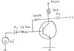
Calculate the following parameter for the given configuration (20)
Q.-5
Calculate the following parameter for the given configuration (20)
1. AI 2. RI 3. RO
4. AV 5. AVS 6. AIS
Q-6. (a) Calculate the element values for a CE transistor at Ic = 1.3 mA (at room temp) at high frequency of operation and draw the model. (10)
(b) Three identical cascaded stages have an overall upper 3-db frequency of 200 kHz and a lower 3-db frequency of 40 kHz. Determine f1 and f2 for each stage. (5)
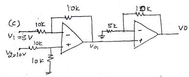
(c) Calculate Vo of the given configuration (5)
Q-7. (a) Calculate ID at VGS= (-1v) for n-channel JFET with the following given data.
ID at VGS =0 is 20Ma and Vp =(-4v) (5)
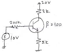
(b) Determine the region of operation for the given configuration (5)
(c) Design an Astable multivibrator using IC555 for pulse generation of 1 kHz having duty cycle of 70%. (c= 10microF) (10)
Q-8 (a) Explain the High frequency model of BJT. Explain each model element and also derive the expression of the fa and fb frequency. (10)
(b) Draw three configuration of BJT and derive the relation between a, b and ,g (gain parameters of the CB, CE and CC) (10)
| Earning: Approval pending. |