Deemed University 2010 B.Tech Electrical and Electronics Engineering University: Lingayas University Term: III Title of the : Electronics Engineering - Question Paper
Roll No. ..
Lingayas University, Faridabad
Examination May, 2010
Course: B.Tech. Year: IInd
Semester: III Paper Code: EE-213E
Subject: Electronics Engineering
[Time: 3 Hours] [Max. Marks: 100]
![]()
Before answering the question, candidate should ensure that they have been supplied the correct and complete question paper. No complaint in this regard, will be entertained after examination.
![]()
Note: Attempt any Five Questions. Draw neat sketches wherever required.
Q-1 (a) Draw the circuit diagram of a full wave rectifier using two diodes and calculate
(i) Idc (ii) Irms (iii) PIV Rating of diode. (15)
(b) Draw the volt-ampere characteristics of ideal diode and explain. (5)
Q-2. (a) In how many modes the BJT works? Also explain the biasing pattern for each of them. (15)
(b) Why CE configuration is most popular in amplifier circuits as compared to CB configuration. (5)
Q-3. (a) What is clipping circuit? Give various configurations of clipping circuits. (15)
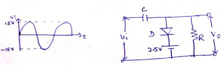
(b) Sketch the output waveform of a clipping circuit shown in the figure by assuming diode is ideal. (5)
Q-4. (a) What are the characteristics of ideal op-amp? Explain the following terms:
(i) CMRR (ii) Virtual ground (10)
(b) Explain how an op-amp can be used as integrator and differentiator. (10)
Q-5. (a) Draw the circuit diagram of a class A transformer coupled power amplifier & explain its operation. Derive an expression for its maximum efficiency. (15)
(b) What is the difference between voltage amplifier and power amplifier? (5)
Q-6. (a) Explain with a neat diagram the working of regulated power supply. (10)
(b) Draw and explain the circuit diagram of op-amp series voltage regulator.
(10)
Q-7. (a) State and prove Demorgans theorem for two input variable. (5)
(b) Convert the following numbers. (5)
(i) (1101101)2 = (?)8
(ii) (11011001)2 = (?)16 (5)
(c) What are universal gates? Why are they called universal gates? (5)
(d) Realize two input EX-OR gate using NAND gates only. (5)
Q-8. Write a short notes on any two of the following. (20)
(i) Load line concept of a diode
(ii) Square wave generator
(iii) Class C power amplifier
(iv) Q point of a transistor.
Roll No. ..
Lingayas University, Faridabad
Examination December, 2009
Course: B.Tech. Year: IInd
Semester: III Paper Code: EE-213E
Subject: Electronics Engineering
[Time: 3 Hours] [Max. Marks: 100]
![]()
Before answering the question, candidate should ensure that they have been supplied the correct and complete question paper. No complaint in this regard, will be entertained after examination.
![]()
Note: Attempt any Five Questions. Draw neat sketches wherever required.
Q-1 (a) Draw the circuit diagram of a full wave rectifier using two diodes and calculate
(i) Idc (ii) Irms (iii) PIV Rating of diode. (15)
(b) Draw the volt-ampere characteristics of ideal diode and explain. (5)
Q-2. (a) In how many modes the BJT works? Also explain the biasing pattern for each of them. (15)
(b) Why CE configuration is most popular in amplifier circuits as compared to CB configuration. (5)
Q-3. (a) What is clipping circuit? Give various configurations of clipping circuits. (15)
(b) Sketch the output waveform of a clipping circuit shown in the figure by assuming diode is ideal. (5)

Q-4. (a) What are the characteristics of ideal op-amp? Explain the following terms:
(i) CMRR (ii) Virtual ground (10)
(b) Explain how an op-amp can be used as integrator and differentiator. (10)
Q-5. (a) Draw the circuit diagram of a class A transformer coupled power amplifier & explain its operation. Derive an expression for its maximum efficiency. (15)
(b) What is the difference between voltage amplifier and power amplifier? (5)
Q-6. (a) Explain with a neat diagram the working of regulated power supply. (10)
(b) Draw and explain the circuit diagram of op-amp series voltage regulator.
(10)
Q-7. (a) State and prove Demorgans theorem for two input variable. (5)
(b) Convert the following numbers. (5)
(i) (1101101)2 = (?)8
(ii) (11011001)2 = (?)16 (5)
(c) What are universal gates? Why are they called universal gates? (5)
(d) Realize two input EX-OR gate using NAND gates only. (5)
Q-8. Write a short notes on any two of the following. (20)
(i) Load line concept of a diode
(ii) Square wave generator
(iii) Class C power amplifier
(iv) Q point of a transistor.
| Earning: Approval pending. |