Thapar University 2007 B.E ELECTRONIC DEVICE AND CIRCUITS - Question Paper
THAPAR UNIVERSITY,PATIALA
B.TECH(DISTANCE EDUCATION),SEPTEMBER 2007
ELECTRONIC DEVICE AND CIRCUITS
B.TECH (DISTANCE EDUCATION) EXAMINATION, SEPTEMBER, 2007
ELECTRONIC DEVICES <& CIRCUITS (EE001D)
TIME ALLOWED: 3 HOURS MAXIMUM MARKS: 100
NOTE: ALL QUESTIONS ARE COMPULSORY.
Ql. (A) Explain the process of Avalanche breakdown. {2 x 10)
(B) How diode is used as a clipper? Explain with the help of neal sketch.
(C) Draw output characteristics of a CB transistor.
(D) How transistor can work as a switch? Explain.
(E) Why the input impedance of a JFET is so high?
(F) Compare B JT, JFET and MOSFET devices in all respect.
(G)Why is class A operation less efficient than class *C operation?
(H)What are the applications of class D amplifier?
(I) Write down the ideal OP-AMP characteristics.
(J) What is the advantage of using high-gain transistor in the phase shift oscillator?
Q2. (A) Derive the efficiency expression of a full wave rectifier circuit (8 x2)
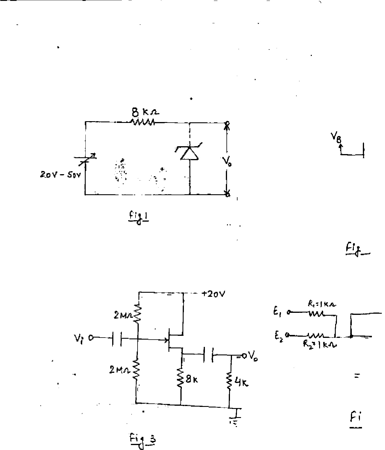
(B) A zener diode of fig (1) has V? =12 V. determine the minimum and maximum zener current as Well as the output voltage, when zener diode is considered to be ideal one.
Q3. (A) The transistor in the circuit of fig (2) has p50 and exhibits a Vbe of 0.7 V. find terminal voltages Vc, VB and Vg, if transistor works in saturation mode.
(B) Draw and explain input-output characteristics of CE transistor.
(8x2)
(8x2)
(8x2)
(8x2)
P.T.O.
Q4. (A) For the JFET amplifier circuit shown in fig (3) if gm = 2500p, and V = SmV, what is the value of Vo.
(B) Explain the working of P-channel JFET.
Q5. (A) Draw a darlington emitter follower. Explain why input impedance is higher than that of a single-stage emitter follower.
(B) Draw the circuit of two stages RC coupled common emitter amplifier and describe the function of each element.
Q6. (A) In fig (4) if E, =10V, Ea = 5V, than Eout =?
(B) Explain the working of crystal oscillator circuit.
|
Attachment: |
| Earning: Approval pending. |