Punjab Technical University 2005 M.Tech Electronics and Communication Engineering Electronic System Design EC 502 - Question Paper
Sunday, 14 April 2013 05:50Web
ELECTRONIC SYSTEM DESIGN EC 502 M Tech first Sem. May 2k5
Max marks 100
Note: Attempt any 5 ques.. All ques. carry equal marks.
1. Realize a full adder circuit using:
(a) 9 Nand Gates
(b) 9 NOR gates
(c) 8:1 Multiplexer
(d) 4:1 Multiplexer.
2. Design a synchronous counter to count in the subsequent sequence:
1,3,5,7,9,11,13,15,1,3,…….
Use J-K flip-flops for realization. Your design should avoid lock out condition.
3. Serial binary data X, synchronized with the clock ,is fed to the logic network shown in Fig. 1. an output will occur on the Z line of the network whenever the string of digits is one 1 01:
4. Using a shift register and combinational logic, design a sequence generator, which will generate the binary sequence: 0-1-0-0-1-0-1-1-1-1-0-1.
5. Design a hazard free D flip-flop using asynchronous circuit design techniques. It may be presumed that the output will take on the value of the input on the trailing edge of a clock pulse.
6. What do you understand by PLA? Draw its block diagram. Realize a full subtractor circuit using PLA.
7. What do you understand by Race around condition? How is it eliminated in Masterslave J-K flip-flop? Draw the block diagram of master-slave flip-flop and discuss its operation.
8. Write short notes on the following:
(a) Shift register
(b) EMC
(c) PAL based design
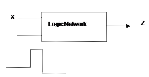
Figure 1

Figure 1
| Earning: Approval pending. |