Anna University Chennai 2003 B.E Mechatronics Engineering Machotronics - Question Paper
D 028
B.E./B.Tech. DEGREE EXAMINATION, APRIL/MAY 2003.
Third Semester
Mechatronics Engineering
EC 154 DIGITAL ELECTRONICS
Time : Three hours Maximum : 100 marks
Answer ALL questions.
PART A (10 2 = 20 marks)
1.
Prove that ![]() .
.
2.
Realize the function ![]() using
only two input NAND gates.
using
only two input NAND gates.
3. Distinguish between EPROM and EEPROM.
4.
Implement the function ![]() using
gates.
using
gates.
5. Draw the symbol and Truth Table for JK flipflop.
6. Define modulus of a counter.
7. What are secondary states (internal states)?
8. How the desired delay is generated in the level mode and pulse mode asynchronous sequential circuits?
9. List the advantages of ASM chart over state graph.
10. What is an SM block?
PART B (5 16 = 80 marks)
11. Draw the ASM chart for a serial sequential adder and explain how the next state and output functions can be synthesized from the chart.
12. (a) Simplify the following function using tabular minimization method.
![]() .
.
Or
(b) (i) Explain how subtraction can be performed
using 2s complement
arithmetic with the help of suitable examples. (8)
(ii) Prove the following :
![]() . (5)
. (5)
(iii) Express the above logic expression in product of sum (POS) form using the duality principle. (3)
13.
(a) (i) Give the Truth table for the full adder and then write
the logic
expression for SUM and carry, and draw the full adder circuit using
gates. Also explain how the full adder circuit can be obtained using
two half adders and OR gate. (8)
(ii) Draw the general structure of programmable logic array (PLA) in block schematic form and explain how it can be used to realize combinational functions. (8)
Or
(b) (i) A single pole double through switch is to be realized using gates. Call the Two inputs of the switch as A and B, a third input C receives the control information in the form of a code 0 or 1. It is desired that C = 0 sets the switch to A and C = 1 sets the switch at B as indicated in the following diagram. Obtain the logic expression for the switch and draw the gate realization. (8)
 |
Diagram for Question No. 13 (b) (i).
(ii) Design a binary to Gray code converter (use 3 bits). (8)
14.
(a) (i) Draw the circuit of a BCD ripple counter and explain
its working
with the help of Timing diagram. (8)
(ii) Draw the circuit of a shift register with the following features :
Parallel load facility, serial left and serial right shift facility and explain its function. (8)
Or
(b) (i) List the advantages of synchronous counter
over that of ripple
counter. (4)
(ii) Explain how the JK flipflop can be made to function as a D flipflop and as a T flipflop. (4)
(iii) Draw the logic diagram of a RAM cell and explain with suitable diagram how the READ and WRITE operation is performed. (8)
15. (a) Minimize the Moore machine shown below and obtain the logic diagram for the machine.
|
|
Next state, Y |
||
|
Present State, y |
Input, x = 0 |
x = 1 |
Output, 2 |
A |
A |
B |
0 |
B |
C |
B |
0 |
C |
C |
D |
1 |
D |
E |
D |
1 |
E |
E |
F |
0 |
F |
G |
F |
0 |
G |
G |
D |
1 |
Table for question 15 (a)
Or
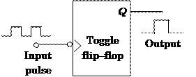
(b) Design a Toggle flipflop whose function table and Input Output waveforms are given below :
 |
|||
 |
|||
Diagram for Question 15 (b)
|
T |
Qt |
Qt+ |
|
0 |
0 |
0 |
|
0 |
1 |
1 |
|
1 |
0 |
1 |
|
1 |
1 |
0 |
Truth Table of T FF
Diagram for Question No. 15 (b)
| Earning: Approval pending. |