Anna University Chennai 2003 B.E Electronics & Communication Engineering Ec 234 — electronic circuits — i - Question Paper
D 032
B.E./B.Tech. DEGREE EXAMINATION, APRIL/MAY 2003.
Third Semester
Electronics and Communication Engineering
EC 234 ELECTRONIC CIRCUITS I
Time : Three hours Maximum : 100 marks
Answer ALL questions.
PART A (10 2 = 20 marks)
1. What are the advantages and disadvantages of fixed bias circuit?
2. What is bias compensation using thermistor?
3. Define the four hparameters.
4. What does bootstrapping mean?
5. What is cross over distortion? How it can be eliminated?
6. Define thermal resistance.
7. What is the relationship between bandwidth and rise time?
8. Draw the frequency response of video amplifier.
9. Define Transformer Utilization factor and ripple factor in half wave rectifier.
10. What is the basic concept of SMPS?
PART B (5 16 = 80 marks)
11. (i) With a neat circuit diagram, explain the operation of transformer coupled class A power amplifier. (8)
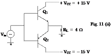
(ii) For the class B complementary A.F. power amplifier shown below, calculate efficiency and maximum power dissipation per transistor. (8)
 |
12. (a) (i) With the help of a neat diagram explain the voltage divider biasing method for JFET. (8)
(ii) Define 3 stability factors. Derive and explain the condition to avoid thermal runaway. (8)
Or
(b) (i) What is meant by bias stability? What
factors affect BJT biasing?
(8)
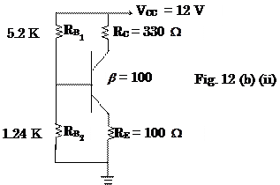
(ii) Draw the dc load line for the following transistor configuration. Obtain the quiescent point. (8)
 |
13. (a) (i) Draw the circuit diagram for a differential amplifier using BJTs. Describe common mode and differential modes of working. (8)
(ii) What is cascode amplifier? Explain. (8)
Or
(b) (i) Derive the expressions for current gain, voltage gain, input impedance and output impedance for an emitter follower circuit. (10)
(ii) Draw a small signal low frequency model for an FET and explain. (6)
14. (a) Discuss the frequency response characteristics of RC coupled amplifiers. Derive the general expressions for gain at low, middle and high frequencies. Draw Bode plots for low and high frequency regions. (16)
Or
(b) (i) Derive the equation for ![]() which gives the relation
between
which gives the relation
between
![]() ,
, ![]() and
temperature. (8)
and
temperature. (8)
(ii) Explain the operation of an optocoupler with a neat circuit diagram. (8)
15.
(a) A half wave rectifier circuit is supplied from 230 V, 50 Hz
supply with a step down ratio of 3 : 1 to resistive load of 10 K![]() . The diode forward resistance
is 75
. The diode forward resistance
is 75![]() while transformer secondary
resistance is 10
while transformer secondary
resistance is 10![]() . Calculate the
maximum, average, RMS value of current, dc output voltage, rectification
efficiency and ripple factor. Derive the formula used. (16)
. Calculate the
maximum, average, RMS value of current, dc output voltage, rectification
efficiency and ripple factor. Derive the formula used. (16)
Or
(b) (i) Derive the expression for ripple factor of
FWR with ![]() section filter.
section filter.
(8)
(ii) Explain the function of switching regulators. (8)
D 032
B.E./B.Tech. DEGREE EXAMINATION, APRIL/MAY 2003.
Third Semester
Electronics and Communication Engineering
EC 234 ELECTRONIC CIRCUITS I
Time : Three hours Maximum : 100 marks
Answer ALL questions.
PART A (10 2 = 20 marks)
1. What are the advantages and disadvantages of fixed bias circuit?
2. What is bias compensation using thermistor?
3. Define the four hparameters.
4. What does bootstrapping mean?
5. What is cross over distortion? How it can be eliminated?
6. Define thermal resistance.
7. What is the relationship between bandwidth and rise time?
8. Draw the frequency response of video amplifier.
9. Define Transformer Utilization factor and ripple factor in half wave rectifier.
10. What is the basic concept of SMPS?
PART B (5 16 = 80 marks)
11. (i) With a neat circuit diagram, explain the operation of transformer coupled class A power amplifier. (8)
(ii) For the class B complementary A.F. power amplifier shown below, calculate efficiency and maximum power dissipation per transistor. (8)
 |
12. (a) (i) With the help of a neat diagram explain the voltage divider biasing method for JFET. (8)
(ii) Define 3 stability factors. Derive and explain the condition to avoid thermal runaway. (8)
Or
(b) (i) What is meant by bias stability? What
factors affect BJT biasing?
(8)
(ii) Draw the dc load line for the following transistor configuration. Obtain the quiescent point. (8)
 |
13. (a) (i) Draw the circuit diagram for a differential amplifier using BJTs. Describe common mode and differential modes of working. (8)
(ii) What is cascode amplifier? Explain. (8)
Or
(b) (i) Derive the expressions for current gain, voltage gain, input impedance and output impedance for an emitter follower circuit. (10)
(ii) Draw a small signal low frequency model for an FET and explain. (6)
14. (a) Discuss the frequency response characteristics of RC coupled amplifiers. Derive the general expressions for gain at low, middle and high frequencies. Draw Bode plots for low and high frequency regions. (16)
Or
(b) (i) Derive the equation for ![]() which gives the relation
between
which gives the relation
between
![]() ,
, ![]() and
temperature. (8)
and
temperature. (8)
(ii) Explain the operation of an optocoupler with a neat circuit diagram. (8)
15.
(a) A half wave rectifier circuit is supplied from 230 V, 50 Hz
supply with a step down ratio of 3 : 1 to resistive load of 10 K![]() . The diode forward resistance
is 75
. The diode forward resistance
is 75![]() while transformer secondary
resistance is 10
while transformer secondary
resistance is 10![]() . Calculate the
maximum, average, RMS value of current, dc output voltage, rectification
efficiency and ripple factor. Derive the formula used. (16)
. Calculate the
maximum, average, RMS value of current, dc output voltage, rectification
efficiency and ripple factor. Derive the formula used. (16)
Or
(b) (i) Derive the expression for ripple factor of
FWR with ![]() section filter.
section filter.
(8)
(ii) Explain the function of switching regulators. (8)
| Earning: Approval pending. |