Bengal Engineering and Science University 2007 B.E Computer Science and Engineering Digital Logic - Question Paper
The ques. paper is with the attachment.
Ex/BESUS/ CST-302(Old)/ 0 7S
B.E. (CST) Part-II 3rd Semester Suppl. Examination, 2007
Full Marks : 100
Time : 3 hours
Answer any FIVE questions, taking at least TWO from each group.
GROUP-A
Draw the truth table for a Half-adder. Implement the half adder using logic gates. Draw the truth table of Full-adder and implement a 4-bit adder with half adders. Extra logic gates, if required, may be used. |20]
1.
a)
b)
|
DATA SELECT | |
 |
OUTPUT OUTPUT |
|
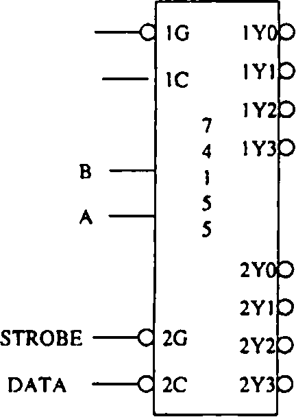
a) 74155 Pindiagram | |
STROBE
| ||||||||||||||||||||||||||||||||||||||||||||||||||||||||||||||||||||
|
b) Function Table for 74155 | ||||||||||||||||||||||||||||||||||||||||||||||||||||||||||||||||||||
Fig.-l [Dual 1 of 4 decoder chip 741SS1
a) Implement full adder logic with dual 2-4 decoder (74155).
2.
b) Implement full adder logic with dual 4 to 1 line multiplexer (74153).
For both the cases (i.e., (a) and (b)) list the number of IC-chips and extra gates necessary to implement 4-bit adders. [20]
|
ISTROBE | |
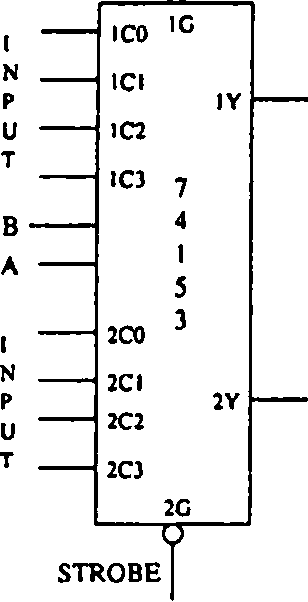 |
OUTPUT OUTPUT |
|
a) Pindiagram | |
| ||||||||||||||||||||||||||||||||||||||||||||||||||||||||||||||||||||||||||||||||||||||||
|
b) Function Table | ||||||||||||||||||||||||||||||||||||||||||||||||||||||||||||||||||||||||||||||||||||||||
Fig.-2 [Dual 4 to 1 multiplexer chip 741531
3. a) Design a combinational circuit using a ROM (8 x 4) that accepts a 3-bit binary
number and produces the square of the corresponding input value. Note that the ROM has eight locations (i.e., 3-bit address) and 4-bit outputs and the square of a 3-bit number is to be expressed in 6 bits.
b) Derive the program table for a combinational circuit to compute the square of a 3-bit number by using PLA. Minimize the number of product terms.
[20]
|
4. a) Design the sequential circuit, whose state table is given below, using a 2-bit register and combinational gates. | ||||||||||||||||||||||||||||||||||||||||||||||||||
|
b) Draw the circuit for a 4-bit bidirectional shift register with parallel load facility. The shift register should have clear and clock inputs as well as two mode control (5j and sQ) inputs. [20]
GROUP-B
5. a) Which logic level limits the fan-out of a TTL gate and why?
b) The output of a DTL inverter is connected to other N number of similar gates. Assume that the output transistor is saturated and hFE of the output transistor is 30. Find the value of N that will keep the transistor in saturation.
c) Compare TTL and CMOS logic families. [20]
6. a) The following logic diagram is used to describe a sequential machine. Draw the state diagram depending on the assumed initial state.
b) Design a 3-bit modulo-6 gray code counter with up/down capability using J-K flip flops.
c) Design a 16:1 MUX using 4:1 MUXs. |20]
7. a) Determine the logic function for the following circuit and explain its operation.
f
+5 V
I
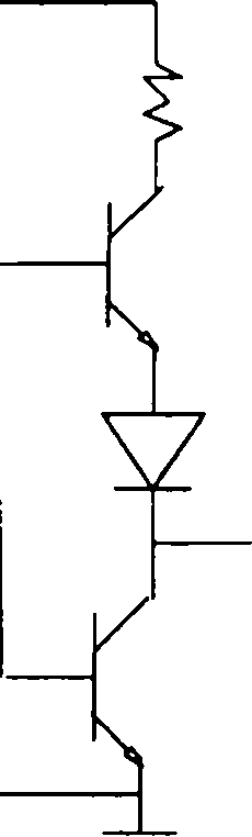
\
b) Use open collector inverter gates to realize the two input exclusive OR function.
c) Define Moore machine and Mealy machine. |20[
8. a) Why cant you make S = 1 and R = 1 in an RS flip-flop? Describe the Race-around problem in level triggered J-K flip-flop,
b) A serial adder uses 2 shift registers and a flip flop. Draw the logic diagram and explain its operation. [20]
|
Attachment: |
| Earning: Approval pending. |