Bengal Engineering and Science University 2006 B.E Electrical Engineering Solid State Devices and Circuits-I - Question Paper
The ques. paper is with the attachment in pdf format.
Ex/BESUS/EE-403/06
B.E. (EE) Part-II 4th Semester Examination, 2006
Use separate answerscript for each half. Answer SIX questions, taking THREE _ from each half. Two marks are reserved_for neatness in each half.
Time : 3 hours
Full Marks : 100
FIRST HALF
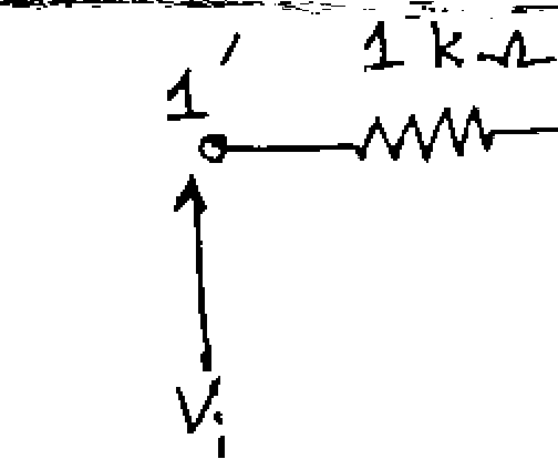
1. a) Find the transfer characteristic of the diode circuit shown in Fig.-1. Consider diode Dl is an ideal diode.
b) If a resistive element of resistance lOkQ is connected across the terminal 1-2, what will be the change in the transfer characteristic.
c) What will be the effect of diode capacitance on the clipping circuit shown in
\
Fig.-l
2. a) Design a full wave bridge rectifier circuit which will convert 220 V, 50 Hz AC input to a DC voltage supplying 50 ohm resistive load.
b) How can you ripple in the output of a rectifier?
c) What is the role of Zener diode in regulating the dc voltage obtained from a rectifier output? [6+4+6]
3. a)
Explain the output characteristic of JFET.
b) A JFET amplifier is shown in Fig.-3. IDSS for the JFET is 1.65 mA and the gate-source pinch-off voltage VP = -2.0 V. Find the voltage amplification.
Assume r<jRL.
(8+8]
m
e
it &
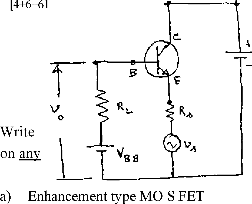
4. a) What do you mean by biasing of a FET?
b) Explain the operation of an universal biasing circuit for FET.
c) A circuit is shown in Fig.-4. Is it an amplifier circuit? Justify your answer.
Vs - input signal
hfe>l
hr
*re
Fig.-4
short notes two :
[8+8]
b) Depletion type MOSFET
c) Peak detector circuit using diodes
d) Voltage multiplier circuit using diodes and capacitors.
6. Express CB h-parameters of a BJT in terms of CC h parameters. Hence evaluate the CB h parameters, if for a typical BJT, it is given that, hjc = 1.1 kQ ; hrc - 1 ; hf = - 51 ; hoc = 25 uA Draw both the h-parameter equivalent circuits. [3x4+4]
a) For the transistor shown the h-parameters with the respect to the E terminal
(i.e., CE h-parameters) are as below hie = 1.1 kQ ; hre = 0.25 x 1(T3 ; hfe = 50; hoe = 2 Find the modified h parameters h'je, h're, h'fe and h'oe . (with respect to the E' terminal) after deriving expressions for the same. Take Re = 1.0 kQ.
7.
|
b) | 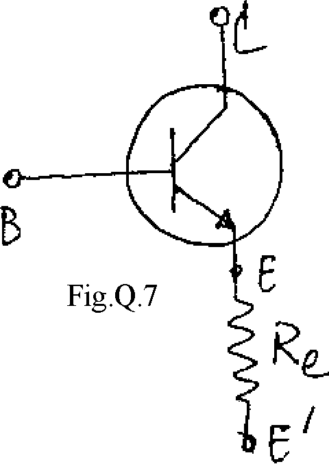 |
and |
From the Taylor series representations of input
characteristics
output
derive the CE-h parameter model of a transistor.
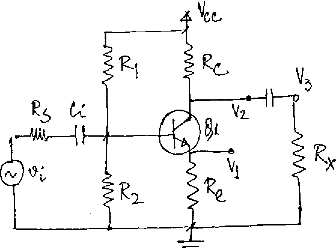
8. a) Identify what
type of circular has been used in the biasing section of the transistor circuit shown in Fig.-9. Derive an expression relating Ic and VBE and discuss the effects of variation of temperature on collector current Ic. How is it better than other biasing schemes?
Derive expressions for the stability factor SI and the stabilisation factors S2 and S3. Discuss about the ranges in which their values may lie.
b)
What are output and input-non-linear distortion with respect to a transistor working as an amplifier? Explain with relevant waveforms. How can distortion be reduced? [5+6+5]
c)
 |
|
Fig.9 For the transistor Ql based circuit in Fig.-9 the nominal point of operation is to be located at Vce - 14V and Ic - 1.6 mA with SI < 4. Assuming that |
9. a)
P - 80, VBE = 0.7 V, Vcc = 18 V and Rc = 3.9 kQ design suitable values of Re, Rj and R2. Evaluate S2 also.
b) If the value of Re as found in part (a) above is set to zero determine (i) the zone of operation of the transistor (ii) the values of Ic, Vj and V2. [9+7]
|
10. a) Identify the component shown by a dashed box in figure Fig.-lO(a). If Vj is a 5.0 V square pulse of 1 kHz frequency |
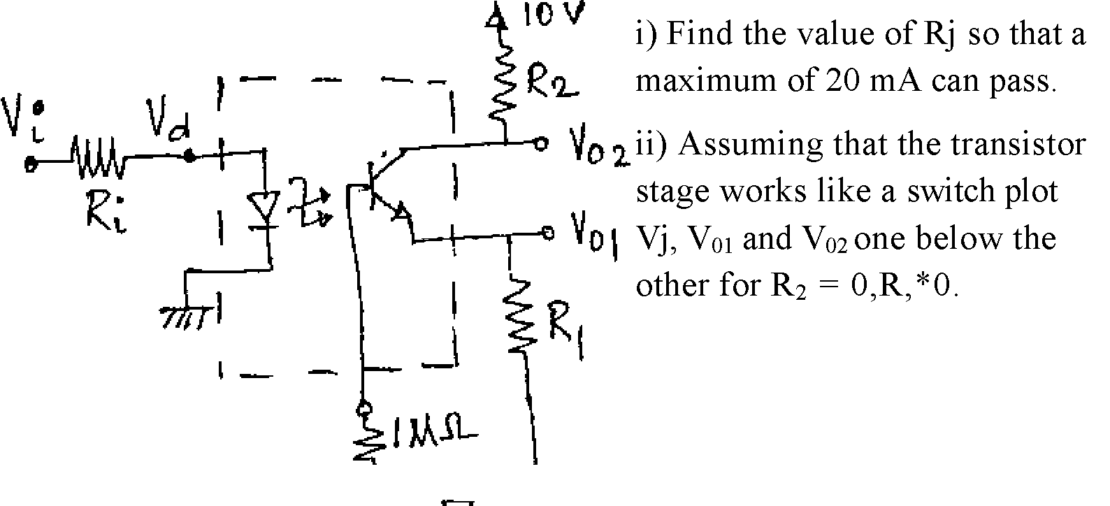 |
iii) Repeat part (ii) for R, = 0 anc* R2*0
Fig.-lO(a)
iv) Plot Vj and V<j against time, assuming reasonable value of diode voltage drop in the on-state.
b) For the schematic connection diagram shown in figure Fig.-lO(b) involving an 1EM Hall Current Sensor determine
i) the recommended pin connections to measure 8-12-25A, with proper justification
ii) the value of the measuring resistance if corresponding to 25 A (r.m.s.) primary current (a.c.) the output voltage has to be around 4.5 V
iii) Principle involved in sensing current.
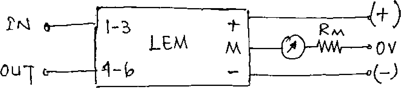
Fig.-lO(b)
The datasheet of the current sensor is as below :
IPN (primary nominal RMS current) = 25 At, IP (primary current measuring range) = 0-55 At, RM (measuring resistance at 70C) = 0 to 155 Q (with 12 V) and 67 to 236 Q (with 15 V). Secondary nominal rms current =
25 mA, Kn (conversion ratio) = 1/2/3:1000, supply voltage = 12 to 15 V.
[9+7]
|
Attachment: |
| Earning: Approval pending. |