Bengal Engineering and Science University 2007 B.E Electrical Engineering Solid State Devices and Circuits-II - Question Paper
Bx/BESUS/ EE-503/07
B.E. (EE) Part-Ill 5th Semester Examination, 2007
S. S. Devices & Ckts.-II (EE-503)
Time : 3 hours Full Marks : 100
Use separate answerscript for each half. Answer SIX questions, taking THREE from each half. Two marks are reserved for neatness in each half.
FIRST HALF
How does the bootstrapping technique increase the input resistance of a CC BJT amplifier? How can the circuit for Darlington BJT CC amplifier in Fig.-l be modified to incorporate bootstrapping circuit?
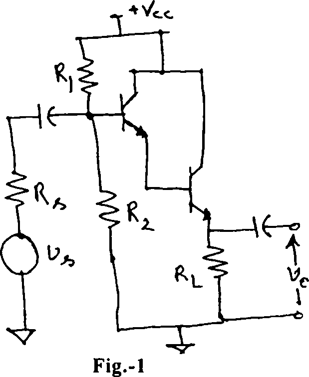
If R,//R2 = 500 kQ , RL = 5 kQ, hfei = hfe2 = 50, hiel = hie2 = 1.5 kQ and l/hoel = l/hoe2 = 20 kQ , find the value of the input resistance Rj without and with bootstrapping circuit. State any assumptions you have made. [5+5+3+3J
A CC circuit is shown in Fig.-2. Find the voltage gain Ay, input resistance R,f
2.
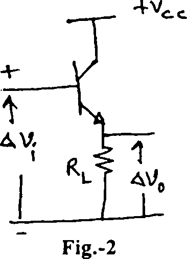
with feedback, the output resistance R0f with feedback using the concept of feedback amplifier. Given hje = 1 kQ , hfe = 100, 1/hoe = 50 kQ and RL = 1 kQ. Biasing circuit is not shown. [6+5+5]
a) Show the basic configuration of a resonant circuit sinusoidal oscillator with feedback.
b) If all the resonant circuit elements are reactive, find at what frequency the circuit will oscillate.
c) Under what conditions does the configuration reduce to a Colpitts Oscillator?
[6+5+5]
4. Design a transformer coupled class-B power amplifier to deliver 30W to a load resistance RL = 4 ohms. Given Vcemax = 80 V , hfe = 100 and hje = 100 Q. Find also the power amplification of the amplifier. How do you modify this circuit to reduce cross-over distortion? [10+3+3]
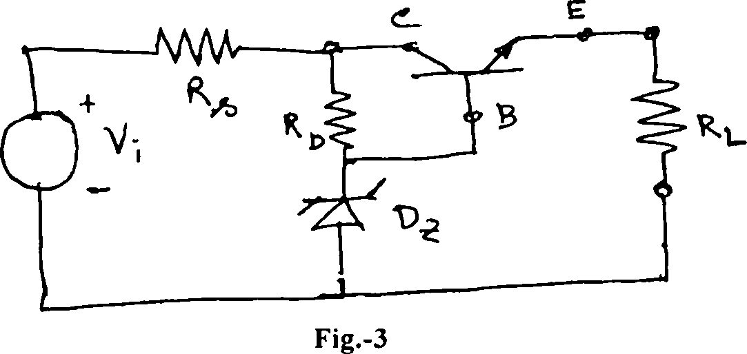
5. For a series regulator as shown in Fig.-3, find the rating of the series transistor and the resistance RD. Given Vj = 18 V 2 V, nominal output voltage equals to 12 V the output current variation from 50 mA to 200 mA, hfe = 50 and hje=100Q at Ic = 200 mA, rz = 12 ohms, Vz can vary between 12.6V to 11.4 V, nominal Vz = 11.7 V. Zener can dissipate 500mW maximum and hfemax = 130. Consider source resistance Rs = 0. Find also R0 and Sv. [10+3+3]
SECOND HALF
6. a) With an introduction to the ideal operational amplifier, draw the adder-cum-
subtracter circuit using op.amp with (2 line + 2 line) inputs and show the deduction of input-output relation.
b) With the help of a circuit diagram, explain the operation of an active integrator circuit and compare it with its passive counterpart. |8+8]
7. a) What is an analog comparator circuit? Show that for sinusoidal input, this
circuit gives a square-wave output by comparing the input signal to ground potential. What is another name of the circuit?
b) What is a regenerative comparator circuit? Show its use as an astable multivibrator and the expression of its frequency of oscillation. [8+8]
8. a) The output (Y) of a digital system is expressed as follows, with usual notation, -
Y(A, B, C, D) = Im (0, 2, 6, 9, 11, 13) + d (4, 5, 7, 8, 10)
Use Karnaugh map and minimise the I/O relation for realisation through NAND-NAND configuration.
b) With the help of circuit diagram, develop a 2-bit comparator circuit with three-bit output Y0, Yj, Y2.
Y0 = 1 , if two input words (A, B) are qual, otherwise O
Y| = 1, if word-A is greater than word-B, otherwise 0
Y2 = 1, if word-B is less than word-B, otherwise 0
Note that Y2 is to be developed using Y0 and Yj. [8+8|
9. a) With the help of block diagrams; truthtable; Venn diagrams; Karnaugh maps
and minterm expressions and maxterm expressions of the output of a full adder circuit. Show that the full adder circuit can be realised using two half adders. Derive the special feature of the gate connecting carry outputs of the half adders to the final carry output of the full adder.
b) What is a MUX? Draw the circuit diagram of a 4-channel MUX using NAND-NAND configuration and use these modules as a full adder. [8+8|
10. Write short notes on any two : [8+8]
a) A differential input differential output amplifier with high input impedance, low output impedance, good CMRR and single gain control facility using not more than two op-amps.
b) Logic circuit of a 2-bit multiplier and 2-bi squarer circuits.
c) Logic circuit of a 4-bit Ripple carry Parallel Adder to add straight binary numbers and development of an 8-bit such adder using above mentioned
4-bit Ripple carry Parallel Adder.
d) TTL NOR gate (2 input) with totempole output and same gate with Open Collector output.
e) CMOS and TTL inverters with 3-state outputs.
f) CMOS MUX-CUM-DMUX circuit (4 channel) for analog and digital signal processing.
4. Design a transformer coupled class-B power amplifier to deliver 30W to a load resistance RL = 4 ohms. Given Vcemax = 80 V , hfe = 100 and hje = 100Q. Find also the power amplification of the amplifier. How do you modify this circuit to reduce cross-over distortion? 110+3+3]
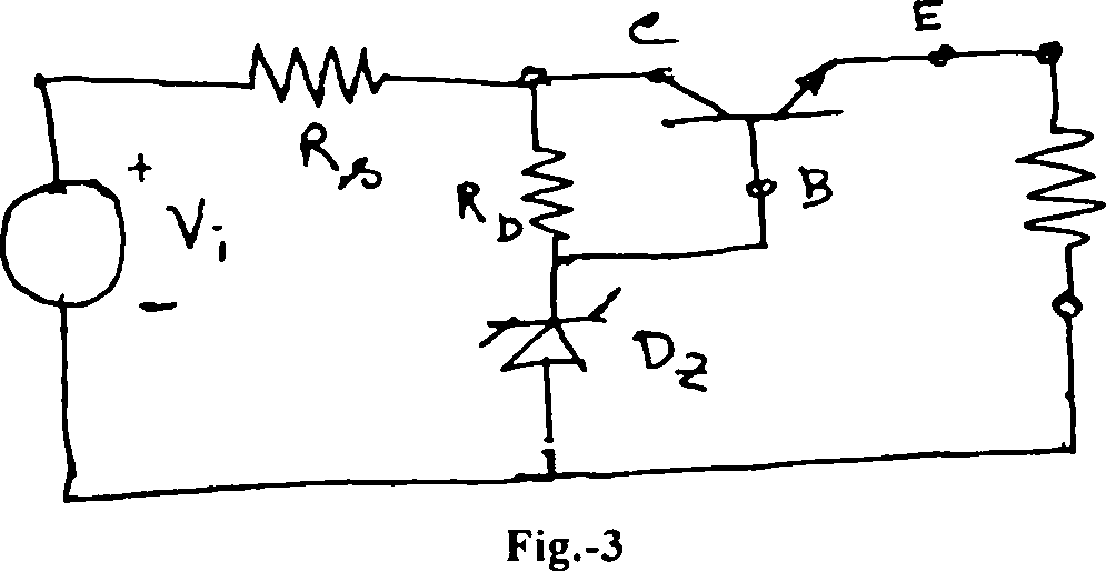
5. For a series regulator as shown in Fig.-3, find the rating of the series transistor and the resistance RD. Given V; = 18 V 2 V, nominal output voltage equals to 12 V the output current variation from 50 mA to 200 mA, hfe = 50 and hje= 100Q at Ic = 200 mA, rz = 12 ohms, Vz can vary between 12.6V to 11.4 V, nominal Vz = 11.7 V. Zener can dissipate 500mW maximum and hfemax = 130. Consider source resistance Rs = 0. Find also R0 and Sv. [10+3+3]
SECOND HALF
6. a) With an introduction to the ideal operational amplifier, draw the adder-cum-
subtracter circuit using op.amp with (2 line + 2 line) inputs and show the deduction of input-output relation.
b) With the help of a circuit diagram, explain the operation of an active integrator circuit and compare it with its passive counterpart. |8+8]
7. a) What is an analog comparator circuit? Show that for sinusoidal input, this
circuit gives a square-wave output by comparing the input signal to ground potential. What is another name of the circuit?
b) What is a regenerative comparator circuit? Show its use as an astable multivibrator and the expression of its frequency of oscillation. (8+8]
8. a) The output (Y) of a digital system is expressed as follows, with usual notation, -
Y(A, B, C, D) = Em (0, 2, 6, 9, 11, 13) + d (4, 5, 7, 8, 10)
Use Karnaugh map and minimise the I/O relation for realisation through NAND-NAND configuration.
|
Attachment: |
| Earning: Approval pending. |